---
robots: index, follow
tags: NCTU, CS, 共筆
description: 交大資工課程學習筆記
lang: zh-tw
dir: ltr
breaks: true
disqus: calee
GA: UA-100433652-1
---
# 數位電路設計----單智君
回目錄
# **第二章 Boolean Algebra and Logic Gates**
1.
- Sum of Minterns
- Product of Masxterms
2. Standard Forms (two level implementsation 兩層電路) -> maybe faster
- Canonical forms
- Standard forms
- Nonstandard form -> maybe cheaper
3. Other logic operations
- all possible functons of n binary variables:
n binary varibles -> 2^n distinct minterms -> 2^2^n possible functions

4. 16 functions subdivided 3 categories
1. 2 functions
2. 4 functions
3. 10 functions
5. Digital Logic Gates
- Boolean expression (AND, OR, NOT)
- Others type
- feasibility and economy
- possibility of extending the gate to more than two inputs
- basic properties
ex.交換律、結合律...
- alone or conjunction
- Gate:
- 0, 1 -> unnecessary
- Transfer, Complement -> y
- Inhibition, Implication -> oppo of upon -> unnecessary
- AND, OR, NAND, NOR, XOR
- NAND and NOR are far more popular than AND and OR

- Extension to multiple inputs
- AND, OR: commutative and associative
- NAND, NOR: commutative but not associative
[(ABC)'*(DE)']' = ABC+DE ≠ (ABCDE)' = A'+B'+C'+D'+E'
- XOR, Equivalence: commutative and associative
- XOR: odd function -> 輸入奇數個 1 時,輸出爲 1
- Equivalence: even function -> 輸入偶數個 1 時,輸出爲 1
- Positive Logic (H = 1) && Negative Logic (H = 0)
同一電路,正負邏輯會使邏輯閘代表意義互補(dual) eg.AND->OR
- Integrated Circuits (ICs)
- Levels (複雜度)
1. SSI small-scale, <10 gates
2. MSI medium-scale, 10~100
3. LSI large-scale, 100~x000
4. VLSI very large-scale, x000~
- Families
1. TTL transistor-transistor logic
2. ECL emitter-coupled logic (speed)
3. MOS metal-oxide semiconductor (density)
4. CMOS complementary MOS (power)
5. basic ckt: NAND, NOR, inverter
- important parameters (additional)
- fan-in (輸入個數)
- fan-out (輸出個數)
- noise margin (辨識度範圍)
- Cost
- propagation delay (輸入出時差)
- power dissipation (
- CAD tools -> Schematic capture tools -> Logic simulator -> Logic synthesizer
# **第三章 Gate-Level Minimization**
1. Introduction and Cost Criteria
- Representation of boolean function (Truth table, Algebraic expression)
- Minimization of boolean function
- Algebraic manipulation: literal minimization -> difficult and hard to sure minimaze
- map method: gate-level minization -> more than 4 variable are hard to use
- Tabular method: Quine-McCluskey method -> systematic producdure
- Cost Criteria
- Two cost criteria:
1. Literal cost: the # of literal apperatances in a Boolean expression
2. ...
- Literal cost:
- the # of literal appenrances in a Boolean expression
- e.g. F = AB+C(D+E) -> 5 literals (non-stander)
F = AB+CD+CE -> 6 literals (stander form)
- Gate input cost (GIC):
- the # of inputs to the gates in the implementation
- good method for conteporary logic implementation
- e.g. G = ABCD + A'B'C'D' -> GIC = 9
G = (A'+B)(B'+C)(C'+D)(D'+A) -> GIC = 12
- For SoP or PoS eqs, GIC = the sum of
- all literal appearances
- the # of terms excluding terms that consist only of a single literal
- the # of distinct complemented single literals operation
2. Map Method
- karnaugh map simplification
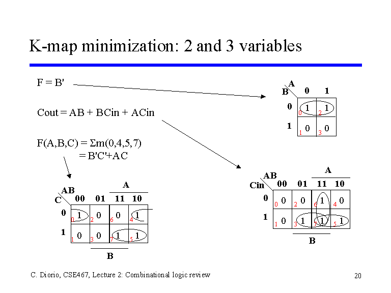

- simple
- k-map: pictorial form of truth table
- n input => 2n squares
- minterm of function
- adjacent squares differ by only one variable
- SOP(sum of products) or POS(products of sum)
- Not unique
- minimum of literals
- minimum of gates
1. Two-Variable
- 2 var -> 2n = 4 minterms
- corresponding minterms have just one var different
- Three-Variable
- 3 var -> 2n = 8
- Find possible adjacent 2k squares:
- each element can used a lot of times
- the most left ele have a ele left next to it is the most right ele
- the most down ele can also cycle to top
- if 1*2 or 2*1 are all 1 -> different ele can be eliminate
- if 2*2 same 1 can also be eliminate
- if 1*4 or 4*1 same
- used bigger rectangle shape is better
1. Four=Variable Map and Five-Variable Map
- Four
- try to make a square
- also can eleminiate by neighbor
- also can left to right or down to top
- eleminiate for 2, 4, 8 (and so on for n-variable)
- used bigger rectangle shape is better
- Prime Implicants
- Implicant
- Prime Implicants (PI): the biggest rectangle for every ele
- Essential Prime Implicants (EPI)
- minterm:
- essential PI
- lest PI choose must selected PI
- deside the minimal cost out of rest of minterms
- Five
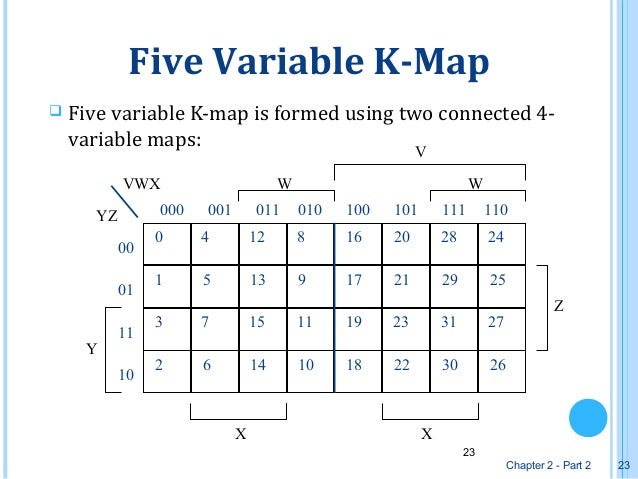

- con
- For upper than 5 var...
1. Product-of-Sum (PoS) Simplification
- using De Morgan's laws after POS of F
- just used POS of F -> 0 and OR
- compare POS and SOP for cheaper
2. Don't-Care Conditions and Quine-McCluskey Method (Tabular Method) (x)
- Don't-Care
- specify with d() = [∑](https://en.wikipedia.org/wiki/Sigma_(letter))m()
- unspecified minterms of a function
- Incompletely specified function specified function
- simplification of an incompletely s
- Quine-McCluskey Method
- finds all PIs and minimum cover of PIs
- used (xy + xy' = x)
1. group by number of 1's
2. compare elements of adjacent groups
- ex:
F(A,B,C,D) = sigma m(0,1,2,5,7,8,9,10,14)

3. NAND and NOR Implementation
- The lest step
- NOT, NAND, NOR is faster
- use NOT, NAND, NOR to make AND, OR, NOT => easier to think
- roles:
1. universal property of NAND gate
1. AND = NAND-NOT
2. OR = NOT-NOR
3. AND-NOT = NOT-OR
4. sop(AND-OR) = NAND-NAND
5. NAND = NOT-OR
2. universal property of NOR gate
1.
4. Other Two-Level Implementations
- Wire logic
- Wired-AND logic: oppen-collector TTL NAND gates
- Wired-OR logic: ECL NOR gates
- 2-level combinations of gates:
- AND OR NAND NOR => 16
- Degenerate forms: 8
- degenerate to dsingle: 2 -> 1 level
- AOI (AND->OR->inverst(NOT))
- F' 的 sum of product
- AND-NOR
- NAND-AND
- OAI (OR->AND->inverst)
- F' 的 product of sum
- OR-NAND
- NOR-OR
5. Exculsive-OR Function
- Exculsive-OR: XOR, ⊕
- x ⊕ 0 = x
- x ⊕ 1 = x'
- x ⊕ x = 0
- x ⊕ x' = 1
- x ⊕ x' = x
- x ⊕ y' = x' ⊕ y = (x ⊕ y)'
- multiple-variable: odd function
- 不相鄰的 2n/2個 1
- 奇數個 input -> output is 1
- 交換率、結合率
- 算 parity bit (b1⊕b2⊕b3⊕...⊕bn = parity bit)
- Exculsive-NOR: XNOR, equivalence
- useful in arithmetic operations and error-detection and correction ckts
6. Multiple-level
- G = ABC + ABD + E + ACF + ADF
- Sop => GIC = 17
- implementation: distributive law
- =>G = AB(C+D) + E + AF(C+D) = A(B+F)(C+D) + E
7. Hardware Description Language (HDL) and Multiple-Level Circuit Optimization
-
# **Verilog Model**
- Hardware description language (HDL)
- feature
- comment: / / or /* */
- file name: .v
- case sensitive
- REMEMBER ' ; '
- Synthesizable Modules & Testbench
- synthesizable modules: describe hardware
- testbench: check output result of module is correct
- Sample of synthesizable modules:
ex:
module Name_Of_Module(inputA,inputB,inputC, outputD,outputE); // module name, parameters for all input and output
output outputD, outputE; // describe output
input inputA, inputB, inputC; // describe input
wire w1; // describe wire
/* GATE following, output is always be the first parameters */
and G1(w1,inputA,inputB); // this is an AND gate, G1 is gate name, w1 is output of gate, inputA and inputB is input
not G2(E,C); // NOT gate, E output, C input
or G3(D, w1, E); // OR gate
/* The order of above gate are NOT important */
endmodule
- Identifiers: case sensitive, name with number, character, _
- comment / / and /* */
- endmodule can without ' ; '
- Sample of testbench:
ex:
module test_bench_name; // no input output
wire C, D; // output
reg A, B; // *input
//instantiate device under test
Name_Of_Module M1(A, B, C, D); // an instantiation of the model to be verified, name of parameters can be difference
// apply inputs one at a time
initial
begin
A=1'b0; B=1'b0; C=1'b0;
#100 A=1'b1; B=1'b1; C=1'b1;
end
initial #200 $finish;
endmodule
- initial statement
- executes the statements in its body at the start of simulation
- should be used only in testbenches for simulator
- \# show as time
- begin, end
- Simulation waveforms (show the result)
- `timescale 1ns/100ps
- ` for compiler directive
- #30 -> 30ns delay
- testbranch
- initial
- begin, end
- $finish
- reg, wire
- boolean exprission
- assign =
- bitwise: & | ~
- logical: && || !
-
# **第四章 組合電路 Combinational Logic**
**gate設計流程:從問題轉成gate的方法:**
1. Specification:確認需要有多少輸入和輸出,並給定各自的symbol
2. Formulation:確認輸入和輸出的關係,畫truth table
3. Optimization:簡化,使用k-map
4. Technology mapping:畫成電路
5. Verification:測試
**binary 加法器:**
半加器(half adder):把2個bit相加
加法器(full adder) :把3個bit相加(實踐起來會是兩個半加器)
### **設計方法:**
- Hierarchical design:
- Top-down
- Bottom-up
- Iterative design
### **加法器 Binary Ripple Carry Adder (n-bit Parallel Adder) (RCA)**
使用Hierarchy & Iterative design,用n個full adder來湊
總共的Propagation-delay是**2n+****1**個gate-delay
但是速度太慢了,所以現實世界不會使用這種設計方法

### **加法器加速方法**
- Carry lookahead:不要等上級給我carry才來算,直接由輸入算出自己的carry
[ ] Carry Lookahead Adder (CLA)
[ ] Gi = Ai Bi: 一定會有carry
[ ] Pi = Ai +Bi: 傳遞的carry跟傳入的carry相同
總共的Propagation-delay固定為**6**個gate-delay

**binary 減法器:**
A - B = A + (1's complement of B) + 1
用一個M來控制加法器的mode
M = 0 => A + B
M = 1 => A + B' + 1

### 處理overflow
- 對於unsigned number:
- 最左邊的bit有carry out就有
- 對於signed number:
- 正加正變負、或負加負變正,就有
- 或是sign bit的carry in⊕carry out為true就有
**十進位加法器:**
- BCD加法器
- 先用正常的adder直接加,需要時做的部分只剩下binary sum轉bcd sum的那一塊
- C = K + Z8Z4 + Z8Z2
- BCD sum = binary sum + 0cc0

**binary 乘法器**
- a*b個AND GATE
- b-1個加法器
- 輸出a+b個bits


**比較器**


**編碼器 encoder**
- 輸入**2^n**個不同的狀況作為訊息
- 編碼成**n**個bit來表示輸入的訊息
- 問題:
- 輸入只能有一個bit是1
- 解決方法:priority encoder,決定輸入的優先順序,哪個先編
- 輸入不能全部是0
- 解決方法:valid-output indicator,新增一個輸出,代表現在的輸入是否有意義
### priority encoder:
優先順序可以任意自訂,這邊的設定為D3優先權最大

**解碼器 decoder**
- 就解碼
- 輸出只會有一個是1
### Line Decoder
- 尾巴加個NOT就可以把minterm轉成maxterm
- active HIGN: minterm
- active LOW: maxterm
- 1-to-2-line decoder

- 2-to-4-line decoder

- 3-to-8-line decoder

### enable input
- 新增一個輸入當成enable input
- 當enable input為正確的值(可能是1或0)時,電路才工作

**Demultiplexer 解多工器(信號分離器)**
- 用來選擇哪一條輸出線會收到資料
- 直接使用line-decoder with enable input來做!
- 只要把enable input當作input data,把data當作線路選擇
任何有n個輸入和m個輸出的boolean function都可以用一個n-to-2^n-line decoder配上m個OR來實作
**Multiplexer 多工器**
- 很多個輸入,選擇使用哪條輸入當作輸出
- multiple-bit selection logic: 多bits資料組的選擇
- 也可以用multiplexer來實作任何boolean function
- 但是multiplexer很貴
- 所以可以用2^n-1的multiplexer來做
- 2^n-2也可以,可是會越來越複雜
**three state gate (tri state gate?)**
- 一般gate的output不可以直接拉在一起,除非有wire-logic,或是保證任何時間只有一個gate output是通的
- Three state gate有兩個輸入:common input和control input
- 當control input是1時,輸出為common input
- 當control input為0時,輸出為0(disabled, 高阻抗?)
- 可以搭配decoder用來實作multiplexer
**組合電路的HDL設計**
- 設計規範:
- 每個模組一個.v檔案,檔名必須和模組名一致
- output要設為module的第一個port
- 三種設計模式:
- gate-level
- dataflow(通常只用在combinational circuit
- behavioral(主要用來做sequential circuit,但也能用來做combinational circuit
- 兩種設計方法:
- buttom-up: 先組小電路,用小電路組大電路
- top-down: 先想大的,需要用到小電路在組小的,大電路較常使用top-down方法
- 系統定義的12個gate:
- 多input單output:
- **and, nand, or, nor, xor, nxor**
- 單input多output:
- **not, buf**
- 四個three state gate:
- active high: **bufif1, notif1**
- active low: **bufif0, notif0**
- 4 value system:
- 各個wire的數值只可能有四種情形
- **0, 1, x**(unknown), **z**(high impedance)
- **output [0: 3] D**:D是一個vector,有**D[0], D[1], D[2], D[3]**四個數,最高的bit(MSB)是**D[0]**
- 2005後的verilog可以將**output, input**的keyword直接寫在module的port list內
- **tri**: 代表那條線路有多個driver(多輸出接在一起的,可能會出現**z**值)
- **wire, wor, wand, tri, supply1, supply0,**多種線的定義
- **dataflow modeling**
- **{ }** concatenation,一次assign多個bits
- **? :** conditional
- dataflow可以簡化很多東西,在合成的時候會根據你下的參數和函式庫設計自動生成對應電路
- **Behavioral modeling**
- **always @**: 符合條件時不斷執行
- 裡面的output要設為**reg**
- @裡面用**or**把各個輸入變數串起來
- 可以寫**always @(*)**,每個變數改變時都會重新run
- 每次@裡面的東西改變時,整個block都會重新run一次
- 設定output值時要用**=**
- **if else**
- **case endcase** **default**
- **casex:** 有x或z時執行
- **casez:** 有z時執行
- 數值表示:N'Bvalue
- **_**可增加數字可讀性,會被編譯器忽略
- **Test Branch**
- 程式進入點:**initial always**
- control flow: **#(Time) repeat(Count)**
- text的方式顯示結果
- **$display**: 會換行的printf
- **$write**: 不會換行的printf
- **$monitor**: 當變數有改變會自動顯示
- **$time**: 顯示時間
- **$finish**
- **%d**: 前面會有空白, **%0d**: 沒有
- **reg wire parameter** 變數
# ch5 Synchronous Sequential Logic
同步電路:有管制改變時間(有閘門)、好設計
非同步電路:沒有管制、速度快、成本低
Latches:非同步,flip-flops的基本
**SR Latch**
- 由兩個NOR組成
- Active **HIGH**
- 兩種正常有用狀態:
- Set: Q = 1, Q' = 0
- Reset: Q = 0, Q' = 1
- 正常的輸入:S,R不能同時為1
- 功能表:
S R Q+
0 0 Q
0 1 0
1 0 1
1 1 不應該發生
**S'R' Latch**
- 由兩個NAND組成
- Active **LOW**的SR Latch
- 功能表:
S R Q+
1 1 Q
1 0 0
0 1 1
0 0 不應該發生
with control
**D Latch**
**moore model vs mealy model**
- moore比較穩定
- mealy反應較快
**HDL**
新關鍵字:**forever**: 無限迴圈
always @(**posedge** wire1, **negedge** wire2)
**<=**: none blocking assignment, 所有 **<=** 會同時做
**電路設計**
狀態減少直接影響flip-flop數量
化簡方法:
- Row matching method
- Implication chart method
# **小考**
 Sign in with Wallet


