# xilinxNote
{%hackmd theme-dark %}
## 索引
## zynq mpsoc 內部結構
https://blog.csdn.net/Archar_Saber/article/details/123588638
http://meseec.ce.rit.edu/551-projects/fall2017/1-7.pdf
https://docs.xilinx.com/r/en-US/ug572-ultrascale-clocking/Introduction-to-UltraScale-Architecture
* I/Os are directly driven from the PHY clocking and/or an adjacent PHY via routing tracks.
* A CMT contains one mixed-mode clock manager (MMCM) and two phase-locked loops (PLLs).
## simu
* [Vivado Design Suite User Guide: Logic Simulation UG900](https://docs.xilinx.com/r/2021.1-English/ug900-vivado-logic-simulation/Supported-Simulators)
* [Writing Efficient Test Benches(XAPP199)](https://docs.xilinx.com/v/u/dITCo7H~owrTV2CvJ8PCuw)
* Post-Synthesis Simulation、Post-Implementation Simulation
RTL simulation沒有時間資訊,Gate level simulation is a simulation of the compiled netlist
* [Vivado的五种仿真模式和区别](https://xilinx.eetrend.com/blog/2023/100570343.html)
1. run behavioral simulaTIon-----行为级仿真,行为级别的仿真通常也说功能仿真。
2. post-synthesis funcTIon simulaTIon-----综合后的功能仿真。
3. post-synthesis TIming simulation-----综合后带时序信息的仿真,综合后带时序信息的仿真比较接近于真实的时序。
4. post-implementation function simulation-----布线后的功能仿真。
5. post-implementation timing simulation-----(布局布线后的仿真) 执行后的时序仿真,该仿真时接近真实的时序波形。
* [IO_and_Clock_Planning](https://leiblog.wang/static/FPGA/books/Vivado%E4%BB%8E%E6%AD%A4%E5%BC%80%E5%A7%8B/Video_10_IO_and_Clock_Planning.pdf)
https://blog.csdn.net/qq_42196515/article/details/114110217
https://xilinx.github.io/xup_fpga_vivado_flow/index.html
```
這邊是XDC檔的片段,可以用來可以用來關掉輸出PORT
set_property OFFCHIP_TERM NONE [get_ports _reg[11]]
set_property OFFCHIP_TERM NONE [get_ports _reg[10]]
set_property OFFCHIP_TERM NONE [get_ports _reg[9]]
# Clock
set_property -dict {PACKAGE_PIN D18 IOSTANDARD LVCMOS33} [get_ports clock]; #50MHz main clock in
set_property -dict {PACKAGE_PIN F22 IOSTANDARD LVCMOS33} [get_ports rst]; #BTN6
# DPY0
set_property IOSTANDARD LVCMOS33 [get_ports seg1[*]]
set_property PACKAGE_PIN F15 [get_ports {seg1[2]}]
set_property PACKAGE_PIN H15 [get_ports {seg1[3]}]
# DPY2
set_property IOSTANDARD LVCMOS33 [get_ports seg2[*]]
set_property PACKAGE_PIN G8 [get_ports {seg2[2]}]
set_property PACKAGE_PIN G7 [get_ports {seg2[3]}]
set_property PACKAGE_PIN G6 [get_ports {seg2[4]}]
set_property PACKAGE_PIN D6 [get_ports {seg2[1]}]
set_property CFGBVS VCCO [current_design]
set_property CONFIG_VOLTAGE 3.3 [current_design]
```
## 參考資料
* 台大ic lab的vivado[介紹](https://hackmd.io/@NTULaDS/S1utFsa9q)(編輯時間2022/07/06)
使用macroblaze建立project,從vivado到vitis圖片很多蠻仔細的,
## xilinx各種UG
### [UG835](https://docs.xilinx.com/r/en-US/ug835-vivado-tcl-commands/Introduction)(Tcl Command Reference Guide)
(如果要用tcl參考UG894,UG835,UG888)
### [UG888](https://docs.xilinx.com/r/en-US/ug888-vivado-design-flows-overview-tutorial/Vivado-Design-Flows-Overview) (Design Flows Overview)
除了講一般ide操作,也有說明no project(tcl)操作方法
####
Vivado% cd <Extract_Dir>/Vivado_Tutorial
Vivado% source create_bft_kintex7_batch.tcl
synth_design -top bft
#### [Step 1: Creating a Project](https://docs.xilinx.com/r/en-US/ug888-vivado-design-flows-overview-tutorial/Step-1-Creating-a-Project)
內文中講的vivado專案模式,就是GUI模式
### [UG892](https://docs.xilinx.com/r/en-US/ug892-vivado-design-flows-overview) (Vivado Design Flows Overview)
一個超級總覽,針對設計流程引出各項細節文件如下
MicroBlaze Processor Embedded Design User Guide (UG1579)
Vivado Design Suite Tutorial: Embedded Processor Hardware Design (UG940)
UltraFast Embedded Design Methodology Guide (UG1046)
如果要用tcl參考UG894,UG835,UG888
UG894(Using Tcl Scripting)
UG835(Tcl Command Reference Guide)
UG888(step-by-step tutorial that shows how to use Tcl in the Vivado tools)
並且還要看project mode,non project mode

#### tcl
1. 啟動vivado tcl mode: `vivado -mode tcl`
2. 或是你可以用批次模式跑你寫的tcl script `vivado -mode batch -source <your_Tcl_script>`
3.
#### Tcl store
[XilinxTCLstore](https://github.com/Xilinx/XilinxTclStore/wiki/Xilinx-Tcl-Store-Home)是一個主要的TCL開源知識庫,但沒有一定要用Xilinx Vivado Design Suite
#### Boardfiles
板子資訊要跟ip integrator做連結,可以參考UG994(IP Subsystems Using IP Integrator),PG169(the Integrated Interlaken up to 150G LogiCORE IP Product Guide)
#### 第三方設計工具
xilinx 合成工具支援新思以及Mentor Graphics使用vivado design suite,但IP與block design 不支援第三方合成
logic simulation支援Mentor Graphics,Cadence,Aldecn,Synopsys.Netlists可以被第三方模擬器產出,你可以輸出tructural netlists with post-implementation delays in standard delay format (SDF)藉由第三方timing 模擬器.
#### I/O planning process
I/O planning process決定FPGA與PCB的關係,關心critical interface routing,location of power rails, and signal integrity.密切的合作可以讓FPGA與PCB設計者可以解決設計問題,IDE可以圖像化看到die pads的位置,並最佳化系統等級的內部連線.
I/O pin可以透過CSV spreadsheet,RTL header,XDC file去包含這些資訊,詳細內容參考UG899,還有這個[目錄](https://docs.xilinx.com/v/u/en-US/dh0007-vivado-pin-planning-hub)
#### ProjectMode
在Vivado IDE當中除了有流程引導外,你順序錯了會幫你事先合成跟implementation.除此之外提供不同策略與觀察點的分析.可參考UG906([Design Analysis and Closure Techniques](https://docs.xilinx.com/r/en-US/ug906-vivado-design-analysis/Introduction))
ProjectMode的優勢:
* 自動管理專案狀態,src,constraint file,ip core,block design
* 生成與儲存合成與實施結果
* 先進的分析能力:cross probing from implementation results to RTL source files
* 自動設定參數去跑策略與標準報告
* 透過設定支援各種跑法
更多細節可參考UG895(System-Level Design Entry)
### UG894 (Using Tcl Scripting)
### [UG895](https://docs.xilinx.com/r/en-US/ug895-vivado-system-level-design-entry/Introduction?tocId=CVFLAAgLj1JTvKXhIvXP9g) (System-Level Design Entry)
* RTL-to-Bitstream Design Flow
*
### [UG896](https://docs.xilinx.com/r/en-US/ug896-vivado-ip/IP-Centric-Design-Flow) (Designing with IP)
### [UG899](https://docs.xilinx.com/r/en-US/ug899-vivado-io-clock-planning/Introduction) (I/O and Clock Planning)
設定pin在對應的die pad上,記憶體設定在指定的i/o bank
### [UG900](https://docs.xilinx.com/r/2021.2-English/ug900-vivado-logic-simulation/Behavioral-Simulation) Logic Simulation
有講到 UNIMACRO
### [UG903](https://docs.xilinx.com/r/en-US/ug903-vivado-using-constraints/Migrating-From-UCF-Constraints-to-XDC-Constraints) Vivado Design Suite User Guide: Using Constraints
For more information on constraints scoping as well as rules, guidelines, and mechanisms for loading the block-level constraints into the top-level design, see this link in the Vivado Design Suite User Guide: Using Constraints (UG903).
### [UG906](https://docs.xilinx.com/r/2021.2-English/ug906-vivado-design-analysis/) (Vivado Design Suite User Guide: Design Analysis and Closure Techniques)
專門在講繞線
* Placement Analysis:
講擺放位置
*
### [UG949](https://docs.xilinx.com/r/en-US/ug949-vivado-design-methodology/Introduction) (UltraFast Design Methodology Guide for FPGAs and SoCs)
* 專注在正確的程式寫法與設計技巧去定義RTL的階層以及Xilinx design constraints (XDC)
* Defining Timing Constraints in Four Steps

### [UG953](https://docs.xilinx.com/r/2021.2-English/ug953-vivado-7series-libraries)(Vivado Design Suite 7 Series FPGA and Zynq-7000 SoC Libraries Guide)
lidar使用的fpga型號,要參考此篇讀相關元件資訊
* Unimacro libary
* FIFO_DUALCLOCK_MACRO
* MMCME2_ADV
Advanced Mixed Mode Clock Manager
* BUFR:
Regional Clock Buffer for I/O and Logic Resources within a Clock Region.

.

### [UG974](https://docs.xilinx.com/r/en-US/ug974-vivado-ultrascale-libraries/Introduction) (UltraScale Architecture Libraries Guide)
對比UG953需要了解zynq mp fpga底層element結構時,參考這篇
### [UG1393](https://docs.xilinx.com/r/en-US/ug1393-vitis-application-acceleration)(Vitis Unified Software Platform Documentation: Application Acceleration Development)
* 如標題,介紹Vitis開發流程,還有XRT加速功能.
* Introduction to Data Center Acceleration for RTL Designers這個段落有講到一些cpu使用RTL加速的方式(但使用Alveo加速卡),核心觀念如下:
* 開發HDL並包成IP
* host app在cpu上跑,透過XRT api寫到的address-mapped register傳到記憶體
* 透過記憶體與alveo上的HDL溝通進行運算
### [UG1483](https://docs.xilinx.com/r/en-US/ug1483-model-composer-sys-gen-user-guide/Overview) (Vitis Model Composer User Guide)
一個用來整合xilinx 跟matlab simulink的圖形化介面
除此之外可以實現DSP功能,並打包做成ip,變成一個submodule
## tcl
https://docs.xilinx.com/r/en-US/ug835-vivado-tcl-commands/Tcl-Shell-Mode
vivado -mode batch -source <your_Tcl_script>
需要先找到一個
## Zynq UltraScale+ MPSoC Embedded Design Methodology Guide ([UG1228](https://docs.xilinx.com/v/u/en-US/ug1228-ultrafast-embedded-design-methodology-guide))
### ch1 introduce
* 四種power domain
* low power domain
* full power
* PL power domain
* Battery power domain
四個電源是分開且隔離,使用PMU管理(Platform mangment unit)
* Vector mathodology diagram

* 向量圖從zynqmp的特性展開並可針對使用情境的特性去評估,以上圖adas的特性來說,需要特性原則就是及時運算,其他電源、儲存媒介、安全性就沒這麼重要,根據需求針對板子去分配資源,也是這份guide想要做的
* block


* RPU
* 32bit operation
* 600mhz
使用 SoC 將處理卸載到 PL 的過程可概括為:
1. 基於硬體功能
2. 最佳化矩陣計算
3. pipeline 效能
4. optimize struture
5. 減少latency
6. improve area
--
評估軟體開發需求
1. Would you prefer running bare metal or using an OS?
2. If you'd prefer bare metal, what are the specific reasons behind this choice?
3. Do you need real-time capabilities?
4. Do you have any boot time constraints? If so, how firm are those?
5. What is your preferred build or development environm
## Vitis High-Level Synthesis User Guide(UG1399)
https://github.com/Xilinx/Vitis-HLS-Introductory-Examples
https://docs.xilinx.com/r/en-US/ug1399-vitis-hls/Mixing-Data-Driven-and-Control-Driven-Models
https://blog.csdn.net/wd1603926823/article/details/125564358
https://github.com/Xilinx/Vitis-Tutorials
https://www.youtube.com/watch?v=kgae3Wzqngs&list=PLo7bVbJhQ6qzK6ELKCm8H_WEzzcr5YXHC&ab_channel=TheDevelopmentChannel
## Design Principles
這個文件主要就是提供一個好的設計原則去合成電路,作為C\C++ 演算法加速的原則
### Throughput(吞吐量) and Performance
Throughput 定義為每單位時間執行的特定操作的數量或每單位時間產生的結果的數量。 這是以每單位時間生產的任何東西(汽車、摩托車、I/O 樣本、內存字、迭代),例如,“記憶體頻寬”有時用於代表記憶體系統的吞吐量, 同樣,性能不僅被定義為更高的吞吐量,而且還被定義為更高的吞吐量和低功耗。 在當今世界,降低功耗與提高吞吐量同樣重要。
### Architecture Matters(架構很重要)
要了解客製硬體如何加速,必須要先了解你的程式是怎麼在傳統硬體上跑的,范紐曼架構可程式化流程主宰了電腦系統七十年,具有multi process,multi thread,達到高吞吐量跟效能。
這樣的系統大量的應用在手機,電腦,遊戲串流...,但現在的挑戰是,怎麼設計一種新的可編成架構,讓你保有足夠的可編程性,同時實現高吞吐量與低電源消耗。
FPGA提供可編程並提供足夠的記憶體頻寬與低功耗的解決方案,不同於CPU跑程式,FPGA提供客製電路來處理需求信號行為,將特出運算映射在裝置上做併行運算
### 三種模式
* 生產者消費者
* 串流資料
* pipeline
### Abstract Parallel Programming Model for HLS
在做平行化之前要先寫出非平行化的程式,去比較改善前改善後
Both blocking and non-blocking read and write semantics are supported for channels, as described in [HLS Stream Library](https://docs.xilinx.com/r/o4VR_92ERnsC86VNmOmjrw/Bj1AYtJD7OOZJM22wSB67g)

### Control and Data Driven Tasks
### h3
A Vitis accelerated application consists of two distinct components: a software program running on a standard processor such as an X86 processor, or ARM embedded processor, and a AMD device binary (xclbin) containing hardware accelerated functions, or kernels.
https://github.com/Xilinx/Vitis-Tutorials/raw/2023.1/Getting_Started/Vitis/images/embedded_processor_flow.png
## Vitis Getting Started Tutorial
https://github.com/Xilinx/Vitis-Tutorials/blob/2023.1/Getting_Started/Vitis/Part4-embedded_platform.md
建立一個嵌入式應用,以vector add做為範例使用G++編譯arm processor,使用v++建立amd device binary(xclbin)

* 軟體模擬:kernel編譯並跑在qemu上,方便debug並快速找出錯誤,使kernel跟app可以一起跑方便觀察行為
* 硬體模擬:kernel便易產生RTL,跑在vivado logic模擬器,app跑在qemu並可以看到動作細節去測試各個功能
* 硬體: kernel code編譯程RTL並放在FPGA
## Building and Running on ZCU102 Zynq MPSoC Embedded Processor Platform
```shell
cd <Path to the cloned repo>/Getting_Started/Vitis/example/zcu102
mkdir sw_emu
cp xrt.ini sw_emu
cp run_sw_emu.sh sw_emu
cd sw_emu
```
進到檔案後根據以下指令編譯
```shell
$CXX -g -std=c++17 -Wall -O0 -fmessage-length=0 ../../src/host.cpp -o ./app.exe -I$SYSROOT/usr/include/xrt -LSYSROOT/usr/lib -lxrt_coreutil -pthread --sysroot=$SYSROOT
v++ -c -t sw_emu --platform xilinx_zcu102_base_202310_1 --config ../../src/zcu102.cfg -k vadd -I../../src ../../src/vadd.cpp -o ./vadd.xo
v++ -l -t sw_emu --platform xilinx_zcu102_base_202310_1 --config ../../src/zcu102.cfg ./vadd.xo -o ./vadd.xclbin
v++ -p -t sw_emu --platform xilinx_zcu102_base_202310_1 --config ../../src/zcu102.cfg ./vadd.xclbin --package.out_dir ./package --package.rootfs ${ROOTFS}/rootfs.ext4 --package.sd_file ${ROOTFS}/Image --package.sd_file ./xrt.ini --package.sd_file ./app.exe --package.sd_file ./vadd.xclbin --package.sd_file ./run_sw_emu.sh
```
V compiler 裡的重要參數
`v++ --package` 產生檔案並包在sd卡上
`emconfigutil`用於 Data Center的模擬環境
....
---
https://www.xilinx.com/developer/articles/acceleration-basics.html
* 以下是用於Data Center的Alveo卡,
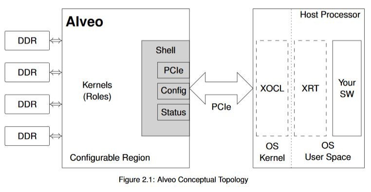
* Alveo cards have multiple on-card DDR4 memories. These memories have a high bandwidth to and from the Alveo device, and in the context of **OpenCL** are collectively referred to as the device global memory
---
https://xilinx.github.io/XRT/master/html/platforms.html
Zynq-7000 and ZYNQ Ultrascale+ MPSoC Based Embedded Platforms

MPSoC Embedded stack

Versal ACAP Embedded stack
https://github.com/Xilinx/Vitis-Tutorials/tree/2023.1/Hardware_Acceleration/Design_Tutorials/04-traveling-salesperson
https://github.com/Xilinx/Vitis_Accel_Examples/tree/master/hello_world
https://github.com/Xilinx/Vitis_Accel_Examples/tree/master
https://docs.xilinx.com/r/en-US/ug1301-getting-started-guide-alveo-accelerator-cards/XRT-and-Deployment-Package-Installation-Procedures-on-\
https://www.boledu.org/textbooks/hls-textbook/application-acceleration-development-flow/host-application-development---xrt
---
https://xilinx.github.io/Alveo-Cards/master/debugging/build/html/docs/common-steps.html#confirm-xrt-platform-compatibility
~~`sudo apt install xrt_<version>.deb`~~
`sudo dpkg -i 軟體套件名.deb`
若相依性有問題使用`sudo apt -f install --fix-missing`
source /opt/xilinx/xrt/setup.sh
---
CPU/GPU/FPGA
Q:甚麼情況用FPGA?
A:大量不規律的平行化運算,客製化的資料型態
Q:FPGA優缺點
A:FPGA的時脈比較受限,但是可以有比較好的擴展性提供比較短的等待時間,因為不用等待高優先權的task
Q:FPGA可以針對客製記憶體需求去做有效率的配置
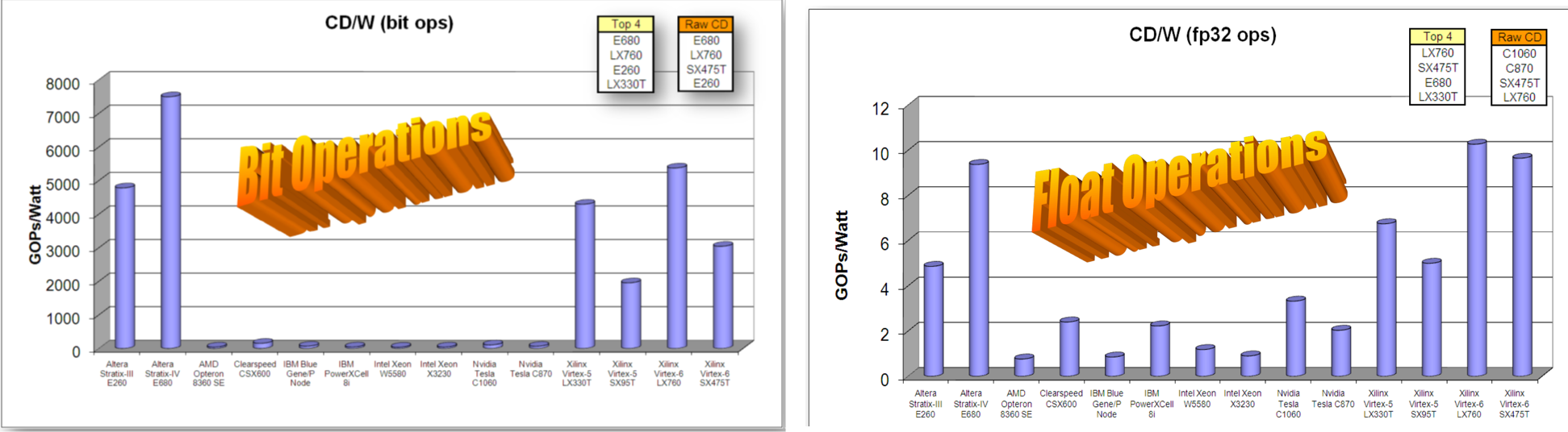
傳統的CPU/GPU會對Fetch跟pipline有較多的能量消耗(這裡是透過比較CD/W(每瓦的運算密度),
有哪些廠商提供相關工具?
* FPGA hardware - offered by FPGA vendor, e.g. Xilinx, Intel/Altera
* The program to be deployed to FPGA
FPGA傳統來說被認為是透過硬體工程師設計,軟體應用加速需要軟體與硬體整合
會阻礙軟體工程師開發的問題
1. 對於RTL當中邏輯閘Level不熟悉會造成無效率
> 使用HLS或opencl提升效率
2. 軟體工程師對於硬體的不了解
3. 當有一部份功能要丟到FPGA需要軟體與硬體溝通的橋樑,需要OS擴增的driver以及API去做溝通與加速
* Coarse-grained :用task在做併行化(thread/fork/TBB)
* Fine-grained:從指令去拆解()
* Instruction-level parallelism
不支援的內容
* system call
* 動態記憶體配置
* 指標限制
* 遞迴
Building Accelerated Applications with Vitis
https://github.com/ATaylorCEngFIET/Building-Accelerated-Applications-with-Vitis/blob/master/
---
Accelerating Deep Learning Models on Xilinx 7nm Versal Card
AI 卡的架構以及實際程式執行流程
https://www.youtube.com/watch?v=FKrR8nHsckQ&ab_channel=AdaptiveComputingDeveloper
xbutil scan
sudo serivce xbutil status
https://www.xilinx.com/products/design-tools/vitis/xrt.html#gettingstarted
 Sign in with Wallet


