###### tags: `TSC` `Linux` `I2C`
I2C 學習
=======
# 介紹
I2C(Inter-Integrated Circuit),中文稱為"兩線式串行總線",是一種廣泛使用的串行匯流排,主要用於嵌入式系統中的微控制器與外部裝置之間的通訊。I2C由飛利浦半導體(現在的恩智浦半導體)在1980年代初開發,具有以下幾個關鍵特點:
簡單的兩條信號線:I2C通訊只需要兩條線,一條是數據線(SDA)和一條時鐘線(SCL)。
多主多從架構:I2C允許多個主裝置(發送命令的裝置)和多個從裝置(接收命令的裝置)在同一條線上共存。
地址化:每個從裝置都有一個唯一的地址,主裝置可以通過地址來選擇與哪個從裝置通信。
同步通信:所有的數據傳輸都是在時鐘信號的控制下進行,確保數據的正確性和時序的一致性。
支持不同的數據傳輸速率:標準模式下最高100 Kbps,快速模式下最高400 Kbps,還有更快的速度,如快速模式加(1 Mbps)和高速模式(3.4 Mbps)。
I2C技術被應用於多種電子設備中,例如在計算機、手機、電視等消費性電子產品中用於連接小型組件如感測器、微控制器等。由於其設計簡潔且有效,能夠支持多裝置之間的連接,I2C成為了許多電子產品和嵌入式系統的首選通訊協議。
> I2C SPEC and i2c-bus.org
https://www.nxp.com/docs/en/application-note/AN10216.pdf
https://www.nxp.com/docs/en/user-guide/UM10204.pdf
Clock Stretching
https://www.i2c-bus.org/clock-stretching/
Fast Mode Plus
https://www.i2c-bus.org/fast-mode-plus/
# I2C lock
當使用 I2C(Inter-Integrated Circuit)通訊協議時,有時可能會遇到稱為「I2C 鎖定」的狀態。這通常是指 I2C 總線被意外鎖定或阻塞,導致數據傳輸無法正常進行。這種情況可以由多種原因引起,以下是一些常見的原因:
- 硬體故障:如果 I2C 總線上的任何裝置發生硬體故障,例如連接線斷裂或接觸不良,可能導致信號無法正確傳輸,進而導致總線鎖定。
- 韌體/軟體問題:錯誤的韌體或軟體邏輯可能導致某個裝置在沒有釋放總線的情況下持續保持控制權,或者在某個操作未完成時就終止通信,這將導致總線無法使用。
- 噪音或電氣干擾:在電氣環境嘈雜的情況下,I2C 總線可能受到干擾,導致數據錯誤或通信中斷。
- 過長的總線線路或過多的裝置:如果 I2C 總線過長或連接的裝置過多,可能會導致信號衰減或反射,增加錯誤率並可能導致總線鎖定。
解決 I2C 鎖定的方法取決於問題的原因,通常包括以下幾種:
- 硬體檢查與修正:檢查所有的連接是否正確無誤,包括線路、接頭和裝置端點。
- 軟體重置:在發生鎖定時,可以通過軟體重置涉及的裝置來嘗試釋放總線。
- 改善總線設計:縮短總線長度,減少連接的裝置數量,使用更適合的拉上電阻,或添加總線隔離裝置。
- 錯誤處理程式:在韌體或軟體中加入錯誤處理機制,如監測並處理未完成的通信操作。
正確地處理這些問題不僅可以解決當前的鎖定問題,還可以預防未來可能的類似事件。
## 改善BUS 電路設計
縮短總線長度,減少連接的裝置數量,使用更適合Pull up電阻,或添加總線隔離裝置。
## I2C pull up Resistance 計算
公式

Rp(max)推導

Example

ref:
I2C Design Mathematics: Capacitance and Resistance:
https://www.allaboutcircuits.com/technical-articles/the-i2c-bus-hardware-implementation-details/
I2C pull up resistor calculation, bus capacitance, and rise time lecture 9
http://fastbitlab.com/i2c-pull-up-resistance-rise-time-and-bus-capacitance-discussion/
教學影片
https://www.youtube.com/watch?v=sGZe0aJsqBQ
https://www.youtube.com/watch?v=CEPFWAPDy7o
先算完再來量, 應該就會接近, 要注意一點, 電容在IC內部若是用類比的方式做, 不同IC誤差很大, 但如果電容是數位模擬的IC, 通常差異不大
教你精确计算 I2C 上拉电阻阻值
https://cloud.tencent.com/developer/article/1916204
https://rheingoldheavy.com/i2c-pull-resistors/
漏极开路上拉电阻取值为何不能很大或很小?
http://www.3ctest.cn/news/show/535
## BUS 電容
NXP 有規範Device IO Pin 的接面電容不可以大於10 pF,我想大部分的device 都會符合這個規範:

1. I2C Bus 除了Pull high 電阻需要警慎使用外, “BUS 電容” 我覺得比Pull high 電阻還重要,因為它不好去確認,而且變數更多。但我們只能有效控制” “BUS 電容”不要太大就已足夠。
==(Rp max 取決於 Cb)==

2. 由於I2C device 是外接,除了IC 本身的接面電容外還有線材上的電容效應,當BUS 上有很多Device 時,電容會越併越大,我們應該注意不能超出 SPEC 的 400 pF (on Fast mode 400Khz)
3. 以下為 SPEC 提出降低電容效應的方法,我列出一些重點以及個人看法

- Reduced fSCL : 降低操作頻率
- Higher drive outputs: 提升軀動能力
- Bus buffers: 使用一個Buffers 準位準態 or 提升軀動能力
- Switched pull-up circuit: 利用電路切換 Pull High 的使用來降低電容效應. (這我不是很懂)

4. 改善 I2C BUS 走線
若大於 10 cm SPEC有建議走線方式,若我們願意使用雙絞線 SPEC建議 SDA 跟SCL 跟Vss 絞在一起 或者 SDA跟 Vdd ; SCL 跟Vss。==我想這可以多少降低一些串擾(crosstalk)以及兩條線之間的電容效應.==

5. 有個看似專門處理 I2C Bus電容過大的IC: LTC4315
[LTC4315 介紹 ](https://www.cytech.com/zh_tw/knowledge/technical-articles/macnica-fae/method-reducing-communication-errors-i2c-bus)
6. 推測 I2C Bus 上的電容.
Rp(max) 的公式是由 RC 充放電的公式推倒而來,而在實際應用下我們已固定Rp ,理論上可以透過量測 Tr 來 推測目前Target board I2C Bus 上的電容.
而理論上 Cb 不應該過大 ( < 400pF on 400khz Fast mode).
`Cb = Tr/ ( 0.8473x Rp)`
[Rp (max) 公式 推導]
[Tr]
[Rp Vs Cb]
而 Rp 在 Fast-mode 下 tr 最大為300 ns, 若預估 Bus 最大電容在 200 pF 以內 (雖然Cb Fast-mode 規範在 400 pF 以下,但實際上超過 200pF 波型應該就不太好), 它適合的 最大阻值 是 1.77 K ohm.

ref:
- CAN總線電容過大的三種解決方案
https://kknews.cc/zh-tw/news/99l24g5.html


### 如何確認哪一個 device 把 I2C Bus 鎖住
我們可以在 MCU (Master) 端 加上一個 Rs 的串阻,然後在 Device (slave) 端也加上一個 串阻,這樣當I2C lock 時 SDA 被拉Low 時可以在一個量測點,量到不同電壓,進而可以判斷是哪邊把腳位拉低.
而Rs 預設可以為 0 ohm ,也可以加些阻抗來抑制一些overshot 。當我們在抓問題的時候可以匹配成適合的阻值,來定位哪個Device 有問題。 或許 某個 device 的 VIL 過高 ,又或者不符合I2C 的SPEC,這個時候可以思考把那個device 獨立一個 I2C Bus 控制,不與其它I2C裝置並接.


### PCB layout 抗干擾設計

https://community.infineon.com/t5/%E7%9F%A5%E8%AF%86%E5%BA%93%E6%96%87%E7%AB%A0/%E4%B8%BA%E4%BB%80%E4%B9%88%E4%B8%B2%E8%A1%8C%E9%80%9A%E4%BF%A1%E7%BA%BF%E8%B7%AF%E4%B8%8A%E9%9C%80%E8%A6%81%E4%B8%B2%E8%81%94%E7%BB%88%E7%AB%AF%E7%94%B5%E9%98%BB-KBA225247/ta-p/258711
https://community.infineon.com/t5/Knowledge-Base-Articles/Need-for-Series-Termination-Resistors-on-Communication-Lines/ta-p/252049

## I2C 軟體重置
### How can I2C lock up?
Now to the problem: in some circumstances the I2C bus can “lock up” in a busy state which prevents the master from ever being able to start a new transaction. Since the master controls the transactions on the bus, this means nothing else can happen after the lock-up occurs. Obviously, this could be a show-stopping condition for any system that depends on the I2C bus to scan sensors or read from EEPROM, for example.
That raises several questions including:
* what causes I2C lock-up?
* how can lock-up be detected and recovered from?
* how can lock-up be prevented?
To understand how the I2C bus can lock up, it’s helpful to think of things from the perspective of a slave device. The slave must monitor the state of the clock and data signals, and in particular must look out for transitions of either signal which may indicate the start or end of a transaction or the need to clock data in and out. All will be well provided the slave device sees the same series of transitions that the master generates, assuming they conform to the I2C protocol specification.
But if there’s some noise or interference that causes an unwanted extra transition or masks a wanted transition, the slave can get out of step with the master. For example, if the master needs to transfer one byte of data from the slave, the slave is expecting to see a specific number of transitions on the clock signal to clock each bit of the data out (and to provide an acknowledge signal). If a clock edge gets “lost” somehow, the slave device will never finish transferring the data and may end up continuously pulling the data line to an active low state.
Now the master might “think” that the transaction has finished, so won’t issue any more clocks, but the slave “thinks” the transaction is still in progress so will keep the bus in a busy state. While the bus is busy, the master can’t generate any more clock transitions. While there are no clock transitions from the master, the slave won’t let go of the bus.
Another situation where lock-ups might occur is during start-up when i/o signals from the master might have glitches or other unexpected transitions before they are stable. If an I2C slave device is monitoring the bus before the master brings the clock and data lines into the right (passive) state, this can cause the I2C bus to be locked before the master starts the first transaction.
Finally, even if the bus is very well-behaved and doesn’t suffer from noise or glitches, lock-up can occur during software development. Let’s say you’re testing and debugging a system using I2C and your software crashes or hits a breakpoint while an I2C transaction is in mid-flight. If you simply reset the CPU or re-start the software, the I2C slave will never see the end of that transaction so the I2C bus will be locked when the software re-starts.
## How should my design handle lock-up?
So, I2C lock-up is definitely “a thing” in practice as well as theory. What can be done about it?
The first approach is prevention. This largely depends on good electronic design to minimise the chance of noise and glitches. For example, this might include:
* using “strong” pull-ups to speed up the rising edge of the SCL and SDA signals
* using i/o signals on the I2C master that have default “high” state, possibly with pull-ups, when the master comes out of reset
Software can sometimes also play a role: if the software running on the master has to configure the signals used by the I2C interface, be careful to make sure that the configuration sequence can’t introduce any unwanted transitions.
Despite the best intentions to prevent lock-up, it’s good practice when designing a system based on I2C to assume that lock-up can occur and to make the system resilient by detecting and recovering from it. This is usually a burden placed on the master software, although hardware design can also help out.
The basic principles here are:
* always implement a well-defined time-out period when waiting for any I2C event
* if a time-out occurs that might indicate a lock-up, either reset all the slave devices or issue a sequence of at least ten clock cycles on the I2C SCL signal
All production-quality I2C device drivers should support time-outs when waiting for I2C events such as gaining access to the bus and completion of data transfers. Depending on the design, the I2C master may include a dedicated controller that might have hardware support for time-outs, in which case the driver should use it. Otherwise, or if the master uses “bit-banged” discrete input/output signals to drive the I2C interface, the I2C driver might have to use software time-outs. Either way, if a time-out occurs it could mean that the I2C bus has locked up and some recovery action needs to be taken. (One exception to this is if you’re dynamically “probing” the I2C bus to discover what devices are on it, but that is not very typical in production software for an embedded system.)
The best recovery action will also depend on the hardware design. In the best case, the hardware will allow each I2C slave device to be reset by the software on the master. For example, this could be done by toggling one or more discrete output signals. Otherwise, the best recovery action is usually to force a series of at least ten clock pulses out on the I2C clock signal. Why ten pulses? Because typically it takes nine clock pulses to clock one data byte in or out of a slave device, after which it will normally release the bus.
If the hardware has a dedicated I2C controller, generating this sequence of pulses might not be straightforward because the controller hardware might not give you direct access to drive the clock signal. In that case, you may have to re-configure the I2C clock pin so that it can be driven as a bit-banged discrete output. In any case, make sure that the clock pulses are generated at about the right frequency (e.g. 100 kHz or 400 kHz), and definitely no faster than the maximum clock rate of any device on the bus.
## How about a real-world example?
Here’s a typical piece of code taken from a system I worked on recently to generate this clock sequence. The master was an NXP KL17 micro-controller, which has a built-in I2C controller. The KL17 I2C controller doesn’t let software drive the clock directly, so I had to configure the SCL signal as a bit-banged output for the recovery sequence, then re-configure it to be used by the I2C controller for normal operation:
```c=
/**
* @brief Definitions
*/
#define I2C_RECOVER_NUM_CLOCKS 10U /* # clock cycles for recovery */
#define I2C_RECOVER_CLOCK_FREQ 50000U /* clock frequency for recovery */
#define I2C_RECOVER_CLOCK_DELAY_US (1000000U / (2U * I2C_RECOVER_CLOCK_FREQ))
...
/**
* @brief Recover I2C from potential lock-up condition
*
* Issue a sequence of ten clock cycles on the I2C SCL i/o pin, without regard
* to the normal I2C protocol. This is intended to recover from a lock-up
* condition whereby a slave is driving SDA low because it is stuck in mid-
* transaction. This condition should not occur during normal start-up from
* power-up, but it may occur if the software is re-started (e.g. during a
* debugging session).
*/
void i2cLockupRecover (void)
{
/*
* Configure SCL pin as GPIO.
*/
PORT_SetPinMux (I2C_SCL_PORT, I2C_SCL_GPIO_PIN, kPORT_MuxAsGpio);
/*
* Initialise pin direction and initial state (high).
*/
const gpio_pin_config_t pinConfig =
{
.pinDirection = kGPIO_DigitalOutput,
.outputLogic = 1U,
};
GPIO_PinInit (I2C_SCL_GPIO_PORT, I2C_SCL_GPIO_PIN, &pinConfig);
/*
* Synthesise several clock cycles; leave i/o pin high.
*/
for (unsigned int i = 0U; i < I2C_RECOVER_NUM_CLOCKS; ++i)
{
delayUs (I2C_RECOVER_CLOCK_DELAY_US);
GPIO_PinWrite (I2C_SCL_GPIO_PORT, I2C_SCL_GPIO_PIN, 0U);
delayUs (I2C_RECOVER_CLOCK_DELAY_US);
GPIO_PinWrite (I2C_SCL_GPIO_PORT, I2C_SCL_GPIO_PIN, 1U);
}
/*
* Reconfigure i/o pin as I2C SCL.
*/
PORT_SetPinMux (I2C_SCL_PORT, I2C_SCL_GPIO_PIN, kPORT_MuxAlt4);
}
```
Another piece of good practice is to always issue the “lock-up recovery” clock sequence when the master software starts up. Then any potential glitches during power-up won’t cause the bus to lock up before things get properly started. This technique can also make life much less frustrating when you’re re-starting a system without power-cycling it – for example, during a debugging session.
Here’s a trace showing the software-generated recovery sequence produced by the code above when the system starts up, shortly followed by the first “real” I2C transaction:
Logic analsyser trace of I2C lock-up recovery

If you’re planning to use I2C in your embedded system design, or are already using it, I hope this has given some insight into the potential for lock-up and how to avoid it, or detect and recover from it. May all your designs be lock-up free.
ref:
- [I2C lock-up: prevention and recovery](https://pebblebay.com/i2c-lock-up-prevention-and-recovery/)
- [Linux I2C 总线驱动恢复机制!](https://blog.csdn.net/junwua/article/details/105239591)
- [linux内核:i2c lock-up恢复机制(SDA线被钳低,软件可以做些什么?)](https://zhuanlan.zhihu.com/p/493161798)
- [Tests:I2C-bus-recovery-write-byte-fix](https://elinux.org/Tests:I2C-bus-recovery-write-byte-fix)
- [Reliable Embedded Systems: Recovering Arduino i2c Bus Lock-ups](https://spellfoundry.com/2020/06/25/reliable-embedded-systems-recovering-arduino-i2c-bus-lock-ups/)
# 如何在 linux 使用 I2C
世平集團代理的NXP i.MX8M Mini多核心應用處理器包含了豐富周邊介面,我們今天來探討如何在Linux上做i2c的除錯。在恩智浦原生Linux BSP Build code完成後就有內建i2c工具,讓開發者可以簡單的利用指令存取i2c周邊裝置的暫存器以便確認CPU端對裝置端讀取是否正常,以便可以縮短整個開發時程。
以下我們使用NXP i.MX8M Mini的開發板及NXP PCF85063TP RTC實時時鐘為各位說明。
## 1. 測試環境
### 硬體跳接:
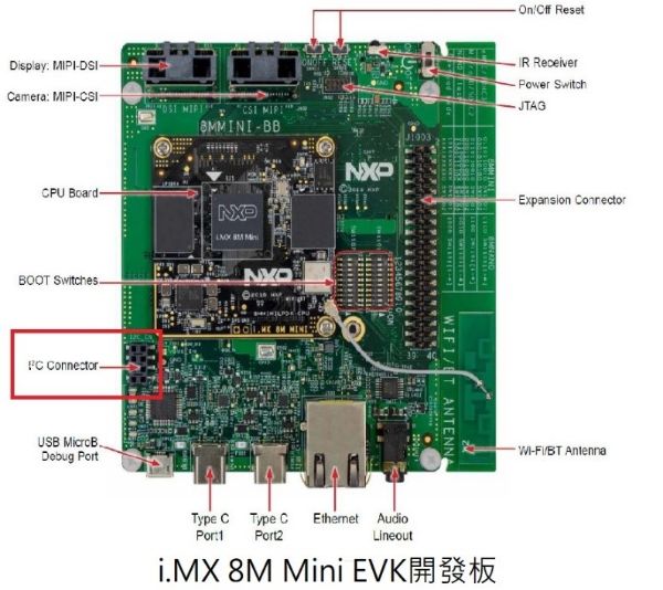
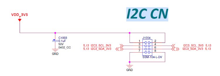
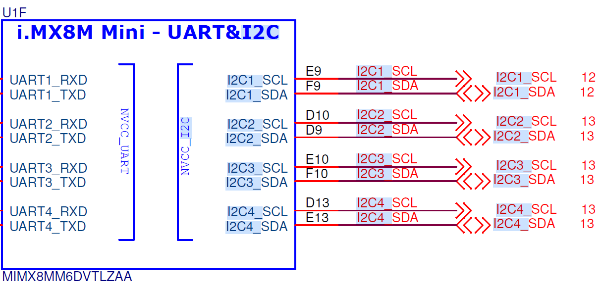
`i.MX 8M Mini EVK開發板的底版上有個I2C CN的Connector線路圖如下:`
我們是使用i.MX8M Mini的I2C3來存取PCF85063TP
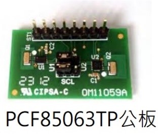
PCF85063TP公板 OM11059A 接腳圖如下:
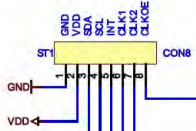
將i.MX 8M Mini EVK開發板及PCF85063TP公板OM11059A的VDD、GND、SDA及SCL相互對接。
i.MX8M Mini 支援四組i2c channel,連接到底板我們是用I2C3跳線到NXPPCF85063TP公板OM11059A。
### 軟體版本:
`使用NXP i.MX BSP Linux 4.19.35_1.1.0作為說明。`
## 2. i2cdetec
1.i2cdetec查看系統上有幾組i2c bus, 輸入i2cdetect -l
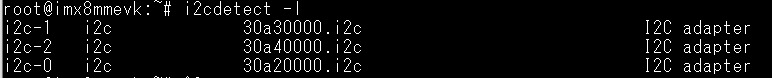
由於在Linux 4.19.35_1.1.0版本的device tree只有設定三組i2c,所以系統用i2cdetec只看到三組。從硬體線路圖來說,第一組i2c是從I2C1開始計數。但是Linux系統上是從i2c-0開始計數,所以我們硬體跳接的I2C3對應到Linux系統為i2c-2。
2.用i2cdetect掃描i2c-2 Bus上的裝置,輸入i2cdetect -r -y 2
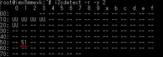
此命令的2代表i2c-2,執行後顯示i2c-2 Bus上有6個裝置,UU表示裝置有被系統偵測到並正在被Kernel佔住。51代表i2c-2上有掃到一個裝置,查看PCF85063TP的datasheet後得知i2c 7-bit address為51
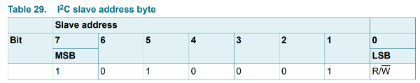
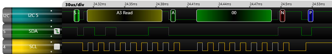
此時我們利用坊間的i2c analyzer擷取Bus上面的波形,若是以8-bit (含read / write bit)顯示的對應關係如下:
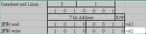
實際波形如下:
## 3. i2cdump
利用i2cdump將裝置上的暫存器的值dump出來。
輸入i2cdump -y 2 0x51:
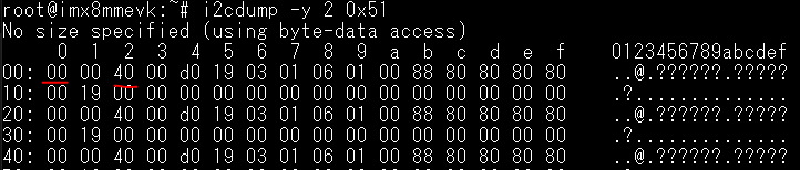
此命令的2代表i2c-2,0x51表示想要讀取的i2c address。
PCF85063TP 暫存器位址0x0的值為0x00

PCF85063TP 暫存器位址0x2的值為0x40
## 4. i2cset / i2cget
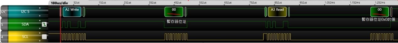
當要設定i2c裝置裡面的某一個暫存器則可以使用 i2cset指令。
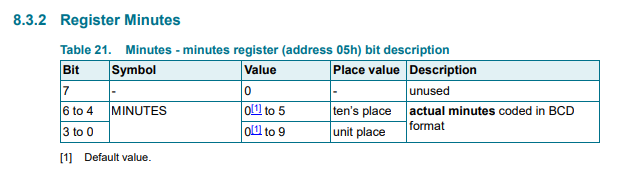
參考PCF85063TP Datasheet得知暫存器位址05是設定分鐘的功能,若要設定為59分鐘的話則輸入i2cset -y 2 0x51 0x05 0x59

此命令的2代表i2c-2,0x51表示想要讀取的i2c address,0x5表示暫存器位址,0x59是要設定暫存器的值。
實際波形:

當要讀取i2c裝置裡面的某一個暫存器則可以使用 i2cget指令。
輸入i2cget -y 2 0x51 0x05

=====================================================================================================
此命令的2代表i2c-2,0x51表示想要讀取的i2c address,0x5表示暫存器位址。返回值為0x59。
實際波形如下:

ref:
- [PCF85063TP](https://www.nxp.com/part/PCF85063TP#/)
- [IMX8](https://www.nxp.com/products/processors-and-microcontrollers/arm-processors/i-mx-applications-processors/i-mx-8-processors/i-mx-8m-mini-arm-cortex-a53-cortex-m4-audio-voice-video:i.MX8MMINI)
- [Linux Tool : i2c-tools 的使用方法, i2cdetect 、 i2cdump、i2cset](https://b8807053.pixnet.net/blog/post/347698301-linux-tool---%3A--i2c-tools-%E7%9A%84%E4%BD%BF%E7%94%A8%E6%96%B9%E6%B3%95%EF%BC%8C-i2cdetect-%E3%80%81-i)
## 其他文章
減少I2C總線通信錯誤的方法
https://www.cytech.com/zh_tw/knowledge/technical-articles/macnica-fae/method-reducing-communication-errors-i2c-bus
彻底搞懂I2C总线(1)什么是I2C?什么是I2C总线?什么是I2C规范
https://zhuanlan.zhihu.com/p/500996257
彻底搞懂I2C总线(2)标准模式、快速模式下的I2C通信协议
https://zhuanlan.zhihu.com/p/509362793
彻底搞懂I2C总线(3)超快速模式下的I2C通信协议
https://zhuanlan.zhihu.com/p/510735588
彻底搞懂I2C总线(4)I2C总线的其他用途
https://zhuanlan.zhihu.com/p/510740723
彻底搞懂IIC总线(5)I2C总线传输速度
https://zhuanlan.zhihu.com/p/510746643
彻底搞懂IIC总线(6)I2C总线电气参数和传输时序
https://zhuanlan.zhihu.com/p/511188270
彻底搞懂IIC总线(7)I2C总线硬件电气连接
https://zhuanlan.zhihu.com/p/512458529
I²C(IIC)总线协议详解—完整版
https://zhuanlan.zhihu.com/p/149364473
掌握总线技术,看这一篇就够了!
https://zhuanlan.zhihu.com/p/136854650
材料介電特性及使用Keysight材料量測方案自動執行介電常數和磁導率量測
https://www.pinsyun.com.tw/content-146.html
TCA39306-Q1 双向 I2C 总线和 SMBus 电压电平转换器
https://www.ti.com.cn/cn/lit/ds/symlink/tca39306-q1.pdf?ts=1684913304944&ref_url=https%253A%252F%252Fwww.google.com%252F
网络分析仪与其他仪器测阻抗的区别?
http://www.utestek.com/news/779.html
由I2C data信号低电平不到0,再思考I2C及GPIO
https://blog.csdn.net/kingsai2012/article/details/124999303?spm=1001.2101.3001.6650.2&depth_1-utm_source=distribute.wap_relevant.none-task-blog-2%7Edefault%7ECTRLIST%7ERate-2-124999303-blog-104671788.237%5Ev3%5Ewap_relevant_t0_download
I2C相关的硬件问题汇总及死锁解决办法
https://www.eet-china.com/mp/a205300.html
I2C总线开发设计需要注意的4个方面
https://blog.csdn.net/qq_21794157/article/details/123906641
I2C接口——I/O级电路设计
https://zhuanlan.zhihu.com/p/561507132
手把手教你写Linux驱动之模拟I2C&e2prom
https://github.com/wfive/simulate_i2c_e2
由I2C高电平不到VCC,再思考时序要求
https://blog.csdn.net/kingsai2012/article/details/129859962

https://www.analog.com/cn/design-notes/hot-swap-and-buffer-i2c-buses.html
https://www.analog.com/cn/parametricsearch/11425#/
http://www.kiaic.com/article/detail/3469.htm
https://www.51cto.com/article/693839.html