###### tags: `introduction of computer`
# 邏輯運算與實現
## 名詞介紹
* 布林代數(Boolean algebra)
能呈現兩種數值(0與1)其中一種的代數形式。
* 訊號邊緣(signal edge)
或稱訊號邊沿,是數位訊號在兩種邏輯準位(0或1)之間狀態的轉變。由於數位訊號準位由方波來表示,因此這種狀態的變化被稱為「邊緣」。
* 競逐狀態
電位輸出訊號不穩定的狀態
* 致能(Enable)
數位邏輯電路要使用與不使用的一個開關。
* 邏輯圖(logic diagram)
電路的圖形表示法。
* 真值表(truth table)
藉由列出所有可能的輸入組合以及相對應的輸出一起來定義閘的功能
* 激勵表(Excitation table)
展示出在已知的現有輸出下,產生出特定的下個狀態所需的最少輸入值
* 狀態轉移表(State transition table)
展示**有限半自動機**或**有限狀態自動機**基於當前狀態和其他輸入,要移動到什麼狀態(或在非確定有限狀態自動機情況下那些狀態)的表格
* VDD、VCC、VSS
在電子電路中
1. VCC是電路的供電電壓:VCC:C=circuit 表示電路的意思,即接入電路的電壓
2. VDD是晶片的工作電壓:VDD:D="device" 表示器件的意思, 即器件內部的工作電壓
3. VSS:S=series 表示公共連線的意思,也就是負極。
在普通的電子電路中,一般Vcc>Vdd !
有些IC 同時有VCC和VDD, 這種器件帶有電壓轉換功能。
在“場效應”即COMS元件中,VDD乃CMOS的漏極引腳,VSS乃CMOS的源極引腳,這是元件引腳符號
*
| 組合邏輯電路 | 順序邏輯電路 |
|:------------------------------------:|:------------------------------------:|
|  |  |
* 時脈
代表處理器一秒鐘可以跑幾個運算單位(GHz:十億,MHz:百萬),所以時脈越高通常代表處理器效能越強
## 使用電晶體(transistir)實現邏輯--閘
### 電晶體(transistor)
* 半導體
1. 純矽晶體- 硼(boron) P-型( positive type)半導體
2. 磷(phosphor) N-型(negative type)半導體
* 電晶體
+ 由半導體製造出來的。電晶體能控制電流的大小和方向,是所有電子裝備的基本元件。製造方法是讓純矽晶體(silicon crystals,屬第四族元素)暴露在高溫的第三族元素(如硼, boron)氣體中,硼元素會藉由擴散進入矽晶體。含硼的矽晶體就變成少了1個電子,也可說多了1個電洞。
+ 硼的角色是受體(acceptor),這就是 P-型( positive type)半導體。如果有第五族元素(如磷, phosphor)的雜質,就多了1個電子。磷的角色是施體( donor),這就是 N-型(negative type)半導體。
+ 經過設計,電晶體可有 3個極,如NPN電晶體有 N-type射極,P-type基極和 N-type集極。
### PNP型電晶體、NPN型電晶體
#### PNP型電晶體
+ 由兩層較厚的P型半導體夾著一層很薄的N型半導體所組成。具有射極(Emitter;簡稱E)、基極(Base;簡稱B)與集極(Collector;簡稱C)三個接腳。PNP型電晶體的結構與電路符號如圖所示。
* 結構圖

* 電路符號

#### NPN型電晶體
+ 由兩層較厚的N型半導體夾著一層很薄的P型半導體所組成。具有射極(Emitter;簡稱E)、基極(Base;簡稱B)與集極(Collector;簡稱C)三個接腳。NPN型電晶體的結構與電路符號如圖所示。
+ 結構圖

+ 電路符號

EX:

### 電晶體如何組成閘
目前製作電晶體主流技術是採用一種稱為「**金氧半場效電晶體**」 (Metal-Oxide-Semiconductor Field-Effect Transistor)的技術,採用這個名稱的原因是因為其中包含一層氧化層,而閘極 (Gate) 上可能會採用金屬作為材質 (但不一定要用金屬)。
因此又可稱 **MOSFET**、**MOS** 電晶體。MOS電晶體主要又分成兩種類型,一種為 **nMOS** 電晶體、一種為 **pMOS** 電晶體。
* pMOS and nMOS
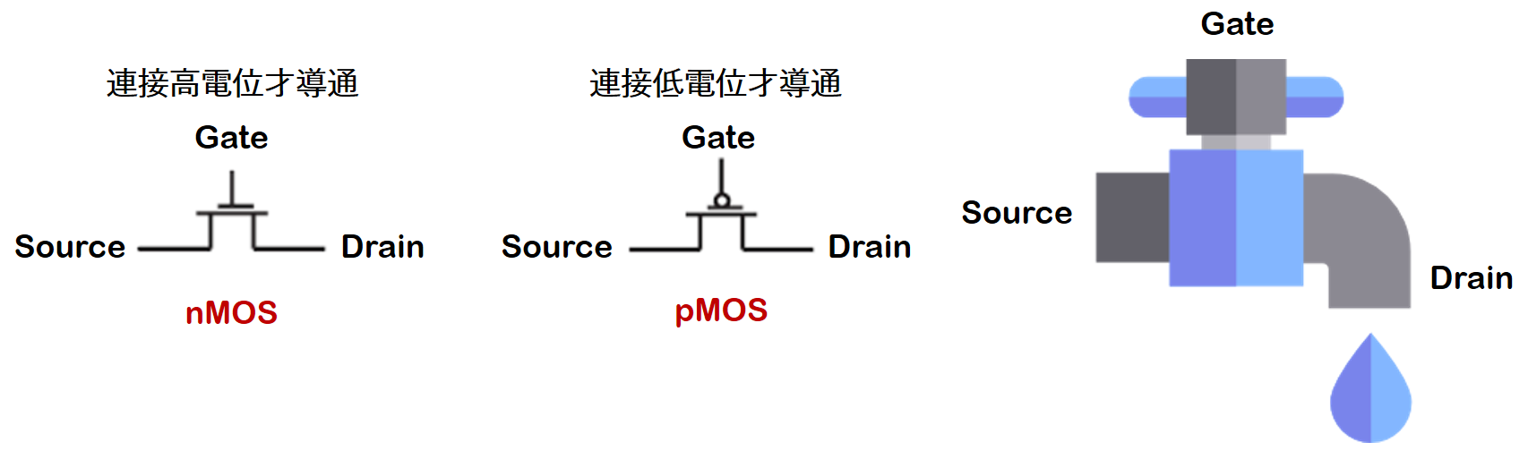
MOS 電晶體對外有三個連接:源極 (Source)、汲極 (Drain) 與閘極 (Gate)。只看這個符號可能會覺得非常抽象,讓我們舉個簡單的例子:
MOS 電晶體的工作原理和水龍頭很類似,電路中的電流就好比水管中的水流,水流的來源就是「Source」、水流出的地方稱為「Drain」,控制水流的水龍頭就是「Gate」。如果把 Gate 打開,電流就會從 Source 流到 Drain,相當於導通電晶體。
如果我們將 nMOS 與 pMOS 兩組功能互相對應的 MOS電晶體組合在一起,就能做出一種非常省電的電路,稱為 CMOS (互補式金屬氧化物半導體, Complementary Metal-Oxide-Semiconductor)。

### 各種閘的操作、原理、表示
| Not gate | 運作原理 |
|:---------------------------------------------------------------------:|:-------------------------------------------------------------------:|
|  |  |
| And gate | And = Not and + Not (this picture is Not and |
|:----------------------------------------------------------------:|:--------------------------------------------------------------------:|
|  |  |
| Xor gate | Xor = not + and + or |
|:--------------------------------:|:------------------------------------:|
|||
* Not gate 的表示法

* And gate 的表示法

* Or gate 的表示法

* Xor gate 的表示法

* Nand gate 的表示法

:::info
Nand gate 可以組合成其他邏輯路線,所以又被稱為萬用邏輯閘
:::
組合電路圖-EX:

## 閂鎖器、正反器
1. 閂鎖器(Latch):
動作時以電壓準位觸發(凖位觸發)或無須觸發訊號即可動作
2. 正反器(Flip okflop(F.F.)):
動作時以訊號邊緣(邊緣觸發)做為觸發訊號


* 正反器可以分成幾種常見的類型:
3. SR (設定-重設,"set-reset")
4. D (資料或延遲,"data" or "delay")
5. T(反轉,"toggle")
6. JK
以上類型的正反器皆可用特徵方程,以現有的輸入、輸出訊號(Q),導出下個(即下個時鐘脈衝的)輸出(Q_{next})。
### RS-閂鎖器、正反器
閂鎖器相關知識
https://reurl.cc/ZOq5kM
R S閂鎖器
https://reurl.cc/KkLYKp
#### RS-閂鎖器
* 有兩種不同的形式
1. 以Nand閘所組成
2. 以Nor閘所組成

* 輸入端與輸出端
* 輸入端
1. R -> reset ->讓$Q$變為'0'
2. s -> set ->讓$Q$變為'1'
* 輸出端
1. $Q$
2. $\overline{Q}$,
(定義$\overline{Q}$為$Q$的反向狀態:$Q=0,\overline{Q}=1 ; Q=1 ,\overline{Q}=0$)
* 利用R、S、$Q_n$、$\overline{Q_n}$去決定$Q_{n}、\overline{Q_{n+1}}$


#### RS-正反器
* **電路圖與電路符號**

* **電路符號接腳說明**

* **真值表推演**

* **真值表**

* **激勵表**

### D-閂鎖器、正反器
#### D-閂鎖器
改良 RS-閂鎖器 再輸入位元同時動作時,會出現違反定義或不確定的情形;因此,可由電路設計來避免產生這種情況,而 **D-型閂鎖器** 就可以改善這個狀況
* **電路圖與電路符號**

* **動作說明**


* **真值表**

#### D-正反器
* **電路圖說明**

* **動作說明**

* **真值表**

* **激勵表**

## 加法器
* 處理二進位加法進位問題
* 圖

### 全加法器

* 全加法器真值表

## 多工器
多工器(Multiplexer)縮寫MUX
* 或稱資料選擇器(Data Selector),功能圖如下,它乃利用資料選擇線S_{o}至 S_{n-1},來選擇資料輸入線D_{o}至D_{2n-1}的其中一條,將此條資料送至輸出端Y。
* 
### 二線對一線多工器
* 電路圖

* 真值表

* 布林函數

### 四線對一線多工器
* 電路圖

* 真值表

+ 布林函數

## 解多工器
解多工器(Demultiplexer)縮寫DMUX
* 或稱資料分配器(Data-Distributor),功能圖如下,它乃利用資料選擇線S_{o}至S_{n-1},來選擇資料輸出端Y_{o}至Y_{2n-1}的其中一條,將輸入資料由此輸出。

### 一線對二線解多工器
* 電路圖

* 真值表

* 布林函數

### 一線對四線解多工器
* 電路圖

* 真值表

* 布林函數

## 解碼器
* 電子技術中的一種多輸入多輸出的組合邏輯電路,負責將二進位代碼翻譯為特定的物件(如邏輯電平等),功能與編碼器相反。解碼器一般分為通用解碼器和數位顯示解碼器兩大類。
* 解碼器可以由**及閘**或**反及閘**來負責輸出。
1. 若使用**及閘**,當所有的輸入均為高電平時,輸出才為高電平,這樣的輸出稱為「高電平有效」的輸出
2. 若使用**反及閘**,則當所有的輸入均為高電平時,輸出才為低電平,這樣的輸出稱為「低電平有效」的輸出。
> 電平
所謂電平,是指兩功率或電壓之比的對數,有時也可用來表示兩電流之比的對數。電平的單位分貝用dB表示。常用的電平有功率電平和電壓電平兩類,它們各自又可分為絕對電平和相對電平兩種。
### 一線對二線解碼器
* 電路圖

* 真值表

* 布林函數

### 二線對四線解碼器
* 電路圖

* 真值表

* 布林函數

### 三線對八線解碼器
* 電路圖

* 真值表

* 布林函數

> 低電位動作輸出(包含效能輸入)
EX: 74138解碼器真值表
* 電路圖

* 符號

* 真值表

* 布林函數

### 四線對十六線解碼器(EX:74154解碼器)
*

* 符號
