# Ch1 GPU 硬體基礎
硬體方面的研究通常是不同設計間的 trade-off
本書主要是在提出這些已經被研究過的設計考量,並提高在非圖形計算類的應用程式的 performance 和 energy efficiency
::: warning
本書內文是作者根據各種不同文獻、專利來敘述,有些細節可能跟實際產品的架構不同,不能盡信
:::
## 1-1 歷史背景
幾十年來,連續幾代計算系統的每美元效能呈指數級增長。根本原因是電晶體尺寸的減少、硬體架構的改進、編譯器技術和演算法的改進
然而,大約自 2005 年以來,電晶體的縮放比例未能遵循 **Dennard Scaling** [Dennard et al., 1974] 規則。所以目前,clock rate 增長的速度緩於裝置變小的速度。
- Dennard scaling:隨著電晶體變得越來越小,它們的功率密度保持不變,所以電晶體尺寸越小,能耗就會成比例的減少,在同個晶片上可以容納更多電晶體,使得裝置可以在不會過熱的情況下執行得更快(clock rate 更高)。
隨著登納德縮放比例定律(Dennard Scaling)的失效,增加能源效率(energy efficiency)是目前計算機架構研究中主要的動力
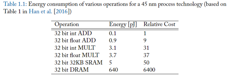
一個重要的觀察結果就是:"存取" 大型儲存結構所消耗的能量,實際上與 "計算" 消耗的能量一樣多,甚至更多。表 1.1 所提供的 45nm 製程中各操作的能量數據 [Han et al., 2016] 就是一個例子。
為了提高性能,需要找到更有效率的硬體架構,下列是一些能夠改善 energy efficiency 的方式:
- hardware specialization
- 使用類似 GPU 的 vector HW,可以減少指令處理的成本
- minimize data movement
- how? 執行複合操作的指令(在避免大型記憶體存取的前提下,可以一次執行多個算術操作)
當前架構面臨的挑戰:效率 vs 彈性:
- 專用硬體通常更有效率,但彈性較差
- 通用型的可以支援更多 program
如果沒有靈活的架構,只有那些能在現有專用硬體上有效執行的演算法才能獲得性能提升,高效運算的範圍被限制在某些特定任務。
雖然有一個趨勢朝向更專用的硬體(機器學習),但總會有對通用計算的需求。
## 1-2 GPU 硬體架構
### GPU 和 CPU 架構的差異
| 特性 | CPU (中央處理單元) | GPU (圖形處理單元) |
| -------------- | --------------------------------------------- | ------------------------------------------------------- |
| **設計焦點** | 針對 sequential code 優化 | 針對浮點計算和 memory bandwidth 優化 |
| **主要任務** | 通用計算任務,包括複雜的邏輯和分支決策 | 圖形處理和高度平行化的計算任務 |
| **硬體架構** | 較少的核心,但每個核心擁有高度優化的性能 | 大量核心,專注於平行處理 |
| **算術單元** | 適合複雜運算,如分支和控制邏輯 | maximize 浮點計算能力 |
| **記憶體** | 大型的 cache 和 memory | 簡化的記憶體系統,通常擁有和需要更高的 memory bandwidth |
| **適用場景** | 適用於高性能單執行緒和快速分支預測的任務 | 適用於需要大規模數據處理和高度平行化的任務 |
| **記憶體頻寬** | 相對較低的 memory bandwidth | 高達 10 倍於 CPU 的 memory bandwidth |
| **設計理念** | latency-oriented,minimize 算術操作的 latency | throughput-oriented,提高整體處理能力 |
### Heterogeneous CPU–GPU System Architecture
A heterogeneous computer system architecture using a GPU and a CPU can be described at a high level by two primary characteristics:
1. how many **functional subsystems** and/or chips are used and what are their interconnection technologies and topology;
2. what **memory subsystems** are available to these functional subsystems.
### GPU 和 CPU 的溝通
目前 GPU 並不是可以 stand-alone computing 的設備,所以考慮的形式是 GPU 和 CPU 進行溝通
- GPU 和 CPU 的通訊
- 目前的 GPU 可能和 CPU 整合在一個晶片上,
- 或是 GPU 插在主機板上透過 PCIE 和 CPU 進行通訊,CPU 用於初始化計算,並且將資料透過 PCIE 匯流排傳入到 GPU 中
- PCIE 通訊速率也是 GPU 的瓶頸之一,因為 PCIE 傳輸對於 GPU 來說太慢了
- GPU 和 CPU 的 I/O
- 目前為止 CPU 中有北橋可以存取 main memory,有中斷器可以對應 input 設備,CPU 還提供了一套 API 去存取 IO,
- 但是 GPU 雖然說做到這些不難, 但是還沒有廠商實現。
- 操作系統也是一個問題,GPU 一般平行處理數據,但是操作系統要求平行處理資料的場景比較少
下面是 CPU 和 GPU 的兩種架構,
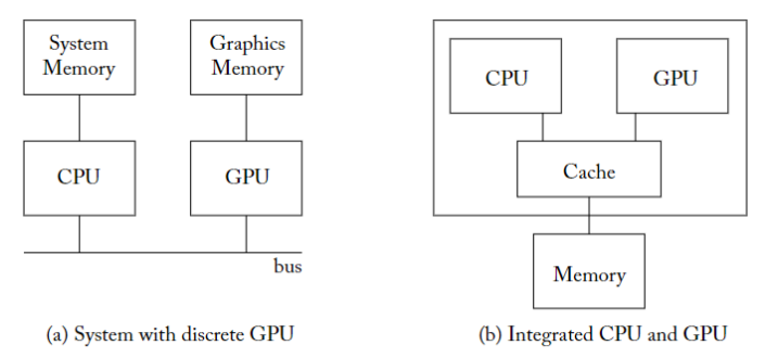
| Device | Memory | DRAM Technology | Optimization |
| ------ | --------------------------- | --------------- | ----------------- |
| CPU | 系統記憶體(system memory) | DDR | Lower latency |
| GPU | 裝置記憶體(device memory) | GDDR | Higher bandwidth |
- 左邊是 GPU 直接插入 PCIE 插槽
- CPU 和 GPU 帶有獨立的 DRAM menory space 和 不同的 DRAM 技術
- CPU 的記憶體通常被稱為系統記憶體(system memory),GPU 的則通常被稱為裝置記憶體(device memory)
- 不同的 DRAM 技術:system memory 使用 DDR ,device memory 使用 GDDR
- CPU 的 DRAM 通常會優先優化 access latency,而 GPU 的 DRAM 則優先優化 throughput
- 右邊是 GPU 和 CPU 整合成一個晶片(AMD 的 APU),只擁有單一的 DRAM 記憶體空間,因此必須使用相同的記憶體技術。
- 由於整合 CPU 和 GPU 的晶片經常出現在低功耗的行動裝置上,因此這種共享的 DRAM 記憶體往往會針對功耗進行最佳化(如 LPDDR)。
### 近代不同的架構設計
- 在 NVIDIA 和 AMD 較舊的獨立 GPU 上,CPU 通常會在 CPU 和 GPU 的 memory space 中,為資料結構分配空間。
- 對於這些 GPU,CPU 執行部分必須協調將 data 從 CPU 記憶體移至 GPU 記憶體。
- 最近的獨立 GPU(如 NVIDIA 的 Pascal 架構),則可透過相關的軟硬體支持,自動地將資料從 CPU 記憶體轉移到 GPU 記憶體中。
- How?
- 這可透過利用 CPU 和 GPU 對虛擬記憶體的支援來實現 [Gelado et al., 2010]。
- NVIDIA 將此稱為「統一記憶體(unified memory)」。
- CPU 和 GPU 被整合在同一晶片,並共享相同記憶體的系統
- 不需要由人來將 GPU 記憶體複製到 GPU 記憶體。然而,由於 CPU 和 GPU 都是用了 cache,並且其中一些 cache 是 private 的,因此這裡可能會出現緩存一致性(cache coherence)的問題,這點需要由硬體開發商來解決 [Power et al., 2013b]。
補充: Basic unified GPU architecture

- **Tesla Architecture**: This design is part of the Tesla architecture, exemplified by the NVIDIA GeForce 8800, which employs a unified architecture. Both traditional graphics programs (vertex, geometry, pixel shading) and computing programs run on these unified SMs and SP cores.
- **Scalability of Architecture**: The processor array architecture can be scaled to smaller or larger GPU configurations by varying the number of multiprocessors and memory partitions.
- **Processor Core Organization**: The GPU architecture contains 112 streaming processor (SP) cores, arranged into 14 streaming multiprocessors (SMs).
- **Multithreading Capability**: Each SP core is highly multithreaded, managing 96 concurrent threads along with their state in hardware.
- **SM Components**: Each Streaming Multiprocessor (SM) includes eight SP cores, two special function units (SFUs), instruction and constant caches, a multithreaded instruction unit, and a shared memory.
- **Interconnection Network**: The processor array is connected to raster operation processors (ROPs), L2 texture caches, external DRAM memories, and system memory via a GPU-wide interconnection network.
- **Texture Processing Units and Cache**: The architecture includes clusters where two SMs share a texture unit and a texture L1 cache. The texture unit supplies filtered results based on texture map coordinates, with the L1 texture cache effectively reducing memory system requests due to overlapping filter regions in successive texture requests.
- **Memory Connection**: The processors are connected to four 64-bit-wide DRAM partitions through an interconnection network.
::: success
怎麼從 CPU 開始呼叫 GPU 進行運算?
:::
### GPU 啟動運算的程序

Part1
- CPU 要先讓 GPU 在 device global memory 上分配空間給"要從 CPU 記憶體搬過去的資料",分配完成後把資料搬過去 GPU 記憶體
- `cudaMalloc`: 呼叫 GPU driver,讓他去在 GPU 上分配記憶體給 program
- `cudaMemcopy`: 把 h_x 指向的CPU memory content,複製給 d_x 指向的 GPU memory
Part2
- CPU 呼叫 kernel (kernel launch),讓 GPU 開始執行運算
- ``kernel <<< M , T >>>``
- a kernel launches with a grid of `M` thread blocks.
- Each thread block has `T` parallel threads.
- 要運行的 kernel、執行緒的數量和資料的位置是由 CPU 上執行的驅動程式(driver)傳遞給 GPU 硬體
- driver 作為中介,將這些資訊轉換為 GPU 可以理解的指令,並將它們放置在 GPU 可存取的記憶體中。
- 隨後,driver 向 GPU 發送訊號,告訴 GPU 要進行新的運算。
Part3
- 把運算結果從 GPU 記憶體回傳給 CPU 記憶體
- 把先前分配的 device global memory 空間釋放掉
- `cudaFree()`: Frees object from device global memory
Example of cuda version of vector addition:


::: success
開始運算後,現代 GPU 常用 SIMT 架構來執行平行化的計算
:::
### SIMT (Single-Instruction, Multiple Threads)
GPU processors are highly multithreaded to achieve several goals:
- Cover the latency of memory loads and texture fetches from DRAM
- Support fine-grained parallel graphics shader programming models
- Support fine-grained parallel computing programming models
- Virtualize the physical processors as threads and thread blocks to provide transparent scalability
- Simplify the parallel programming model to writing a serial program for one thread
what: A processor architecture that applies one instruction to multiple independent threads in parallel.
- 使 GPU 能夠平行執行許多 thread,使其在可以分解為許多同時進行的小操作
- NVIDIA 將這些 core 稱為串流多處理器(SM, streaming multiprocessor),AMD 則將它們稱為運算單元(compute unit)
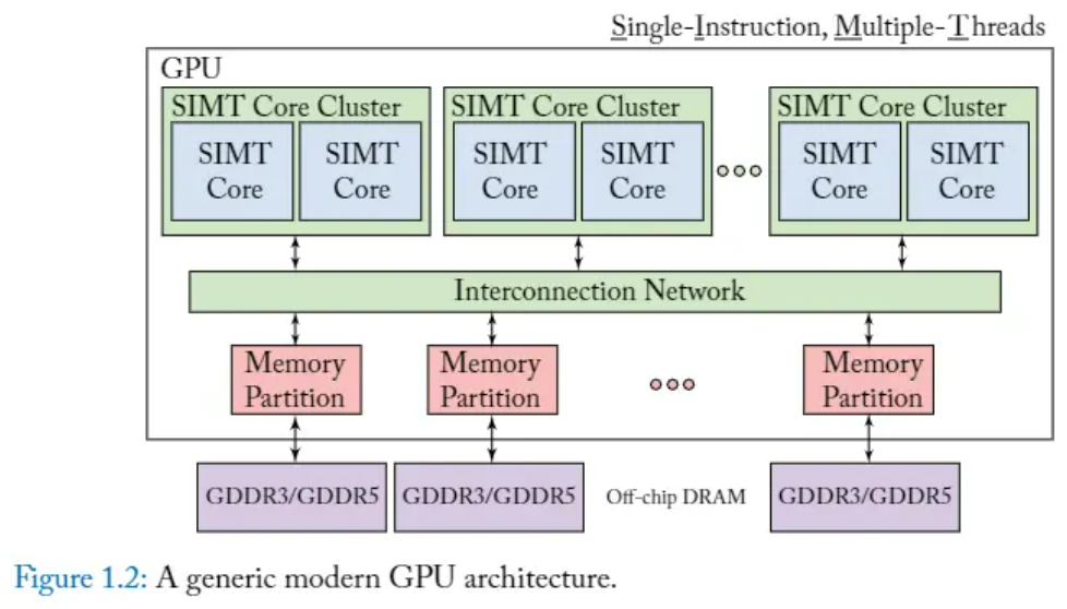
**SIMT Core Cluster**
- What?
- 這是多個 SIMT core 的分組。
- 可以同時使用相同指令但不同資料,來執行多個 Threads。
- Why?
- 這在圖形處理中特別有用,因為同一操作通常應用於許多像素或頂點。
**SIMT core**
- What?
- 每個 SIMT core 能夠同時執行多個(數千個)執行緒,為高度平行的設計,這對於通常由 GPU 處理的大規模平行工作負載來說是理想的。
**Memory Partition(記憶體分區):**
- What?
- GPU 中的記憶體被分成多個分割區(Partition),允許多個 SIMT core 同時存取。
- Why?
- 這種分割對於保持高吞吐量至關重要,因為它最小化了記憶體存取瓶頸
- 如果所有 core 都存取單一記憶體池,將會發生記憶體存取瓶頸。
**Interconnection Network:**
- What?
- 這是連接 SIMT Core Cluster 與 Memory Partition 的 data pathway。它被設計成能夠處理高 bandwidth ,以實現快速數據交換
- Why?
- 這對於維持 core 性能和記憶體訪問效率至關重要。
::: success
從更上層的視角來看整個 GPU 的內部架構:
:::
### GPU 內部架構:
Why? 在 thread 之間以不高的成本快速切換(context switch),是 GPU 維持高使用率和效率的關鍵
- GPU 計算非常快,速度慢的瓶頸是 memory access,所以會不斷 context switch,達到 **隱藏延遲** 的效果(hide memory access latency)
- 一個 core 中可以讓很多 threads 共用,其中一個 thread 如果要進行 memory access,就可以觸發 context switch,讓另一個 thread 來使用,以達到 hide (memory access) latency 的功能
- CUDA 中,每個 thread 都有自己的 **register set**,所以 context switch 時基本上不用動到 register 裡面的值
How? 這些 GPU cores 將負責執行在 GPU 上啟動的 kernel 程序,以單指令多執行緒(SIMT)的方式執行,所以 GPU 上的每個 core 通常可以運行上千個 threads。
- 同處在單一 core 上執行的 threads
- 可透過草稿記憶體(scratchpad memory, shared, fast-access memory area)來溝通
- 可以透過一些高速屏障操作(barrier operations)進行同步。
- 每個 core 內部通常也會包含 L1 instruction cache 和 L1 data cache,可充當 bandwidth filter 以減少到較低階記憶體系統的通訊量。
- 高水準的計算吞吐量( high computational throughput ),有必要和 high memory bandwidth 間進行平衡。high memory bandwidth 很重要,因為它能夠讓 GPU 快速 load 和 store 計算所需的大量資料。
為了達到這種平衡,我們在記憶體系統加入平行性(parallelism),通過以下架構特點實現:
**Multiple Memory Channels**:
- 主記憶體會被切成多個記憶體分區(memory partisions),每個 Partision 會連結到一個記憶體通道(memory channel)
- 在 GPU 中,這種平行性是由 GPU 所包含的多個 memory channel 提供的
- 每個 channel 都是一個獨立的路徑,用於 data 在 memory 和 GPU core 之間的流動。
- 所以通過擁有多個 channel,GPU 可以同時處理更多的 data,從而增加了可供 GPU core 使用的總體 memory bandwidth
**Last-Level Cache Association**:
> Last level cache (LLC) refers to **the highest-numbered cache that is accessed by the cores prior to fetching from memory**. Usually, LLC is shared by all the cores. In Skylake and Cascade Lake, the LLC is the shared L3 cache.
- 每個 memory channels 都會和一部分的 LLC 連結
**On-Chip Interconnection Network**:
GPU core 透過 on-chip network,如 crossbar,來與 memory partisions 連接。
- 其它架構也是可能的,例如在超算市場上與 GPU 直接競爭的 Intel 的 Xeon Phi,就將 LLC 分配給了各個 core
::: success
重點關注 core 和 thread 之間的關係
:::
### 架構分析(core, thread)
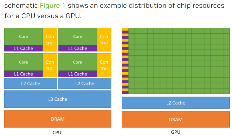
與 CPU 相比,GPU 可將其晶片面積中的更大部分用於 ALU(arithmetic logic units),並減少用於控制邏輯的面積,從而獲得更好的單位面積性能(performance per unit area)。
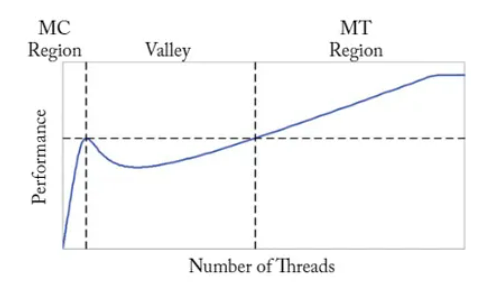
> 圖 1.3,對多核心(MC)CPU 架構和多執行緒(MT)架構(如 GPU)間的效能權衡的模型分析表明,如果執行緒數量不足以覆蓋 off-chip memory 的 memory access latency,就會出現「效能谷( performance valley)」(基於 Guz et al.[2009] 的 Figure 1)
為幫助對 CPU 和 GPU 架構間的權衡有一個直觀的認識,Guz 等人(Guz et al. [2009])開發了一個分析模型,以顯示性能是如何隨 thread 數量的變化而變化的。
模型前提:
- thread 不會共享資料,
- 擁有無限的 off-chip memory bandwidth
圖 1.3 就再現了它們論文中的一個圖表,顯示了他們在模型中發現的一個有趣的 trade-off:
- 當一個大 cache 被少量 thread 共享時(如多核 CPU 的情況),效能將隨 thread 數量的增加而增加(MC Region)。
- 但是,一旦 thread 數量增加到 cache 無法容納整個工作集(working set,在 windows 中用到的 bytes)時,就會達到 Valley,效能下降。
- 然後,隨著 thread 的進一步增加,多 技術也能隱藏較長的 off-chip latency,因此效能隨之提升(MT Region),即透過多執行緒來 tolerate 頻繁的 cache-miss。
### GPU 的歷史要點:
1. **Origins in the 1960s**: Computer graphics technology dates back to the 1960s, marked by pioneering projects like Ivan Sutherland’s Sketchpad.起源於 1960 年代:電腦圖形技術可以追溯到 1960 年代,以伊凡·薩瑟蘭的 Sketchpad 等開創性項目為標誌。
2. **Early Role in Animation and Gaming**: Graphics have played a crucial role in both off-line rendering for film animation and the development of real-time rendering for video games.早期在動畫和遊戲中的角色:圖形在電影動畫的離線渲染和視頻遊戲的實時渲染的發展中都扮演著至關重要的角色。
3. **Evolution of Video Cards**: The progression started with text-only support in IBM's MDA in 1981, followed by 2D and then 3D acceleration, which also benefited computer-aided design.顯示卡的演進:這個進程始於 1981 年 IBM 的 MDA 只支援文字,接著發展到 2D 和 3D 加速,同時也對電腦輔助設計有所裨益。
4. **Advancements in GPU Functionality**: Early 3D graphics processors, like the NVIDIA GeForce 256, were mostly fixed-function. NVIDIA later introduced programmability with vertex and pixel shaders in 2001.GPU 功能的進步:早期的 3D 圖形處理器,如 NVIDIA GeForce 256,大多是固定功能的。NVIDIA 在 2001 年後引入了頂點和像素著色器的可編程功能。
5. **General-Purpose Computing on GPUs**: Researchers found ways to use early GPUs for linear algebra, which led to more general-purpose computing applications on GPUs. NVIDIA's GeForce 8 Series was the first commercial product to support this directly.研究人員發現了如何利用早期的 GPU 進行線性代數運算,這導致了更多通用計算應用在 GPU 上的出現。NVIDIA 的 GeForce 8 系列是第一個直接支援這一功能的商業產品。
6. **Innovations in GPU Architecture**: The GeForce 8 Series added the ability to write to arbitrary memory addresses and introduced scratchpad memory. NVIDIA's Fermi architecture later enabled caching of read-write data.GPU 架構的創新:GeForce 8 系列增加了對任意記憶體地址的寫入能力,並引入了暫存記憶體。NVIDIA 的 Fermi 架構後來實現了讀寫數據的緩存。
7. **Integration and Dynamic Parallelism**: AMD's Fusion architecture integrated the CPU and GPU on the same die. Dynamic parallelism was introduced, allowing for threads to be launched directly from the GPU.整合和動態平行處理:AMD 的 Fusion 架構將 CPU 和 GPU 整合在同一晶片上。引入了動態平行處理,允許直接從 GPU 啟動執行緒。
8. **Machine Learning Acceleration**: The latest innovations, like NVIDIA’s Volta, include Tensor Cores designed specifically for machine learning acceleration.機器學習加速:最新的創新,如 NVIDIA 的 Volta,包括專為機器學習加速而設計的 Tensor Cores。
# Reference:
- Aamodt, T. M., Fung, W. W. L., & Rogers, T. G. 2018. General-Purpose Graphics Processor Architectures. Morgan & Claypool Publishers.
- Hwu, W. W., Kirk, D. B., El Hajj, I. 2023. Programming Massively Parallel Processors: A Hands-on Approach. Morgan Kaufmann.
- David A. Patterson and John L. Hennessy. 2017. Computer Organization and Design RISC-V Edition: The Hardware Software Interface (1st. ed.). Morgan Kaufmann Publishers Inc., San Francisco, CA, USA.
 Sign in with Wallet
Connect another wallet
Sign in with Wallet
Connect another wallet