# 自已的開發板自己做工作坊 ## 裸線焊接你的Atmega328p迷你開發板 [工作訪計畫書_hackmd](https://hackmd.io/4ialXZNIRGWbu7fYnHaSIw?both) [單層板設計_kicad_github](https://github.com/chenlotung/atmega328pSmallest_EVB) - kicad 3d模型圖 -  # 所需材料(粗估成本:每份230元不含運,不含uno板及焊接工具) - [ ] arduino uno r3 開發板 - [ ] cp2102 usb to ttl 模組 - [ ] atmega328p dip 28pin - [ ] 5x7cm以上,單面或雙面玻纖萬孔板 - [ ] 16MHZ 石英震盪器 - [ ] 18-22pF陶瓷電容*2 - [ ] 長杜邦針or母座*28 - [ ] 5mmLED - [ ] 5X6mm直插式按鈕*2 - [ ] 電阻(下列各一) - 1k,1M.10M - [ ] 鍍錫裸線 - [ ] 焊錫 # 實驗步驟 1. 元件測試 - led、按鈕通斷測試 - 電容值電阻值紀錄 - 使用麵包板與uno燒錄bootloader 確認晶片功能正常 定位各元件位置,(參照參考資料之位置圖與走線圖) 未完待續................... 未完成項目:底座製圖(四角拔模圓柱,矩形底座) # 參考資料 ## 照片 - atmega328p pin out   - arduino uno r3 schematic 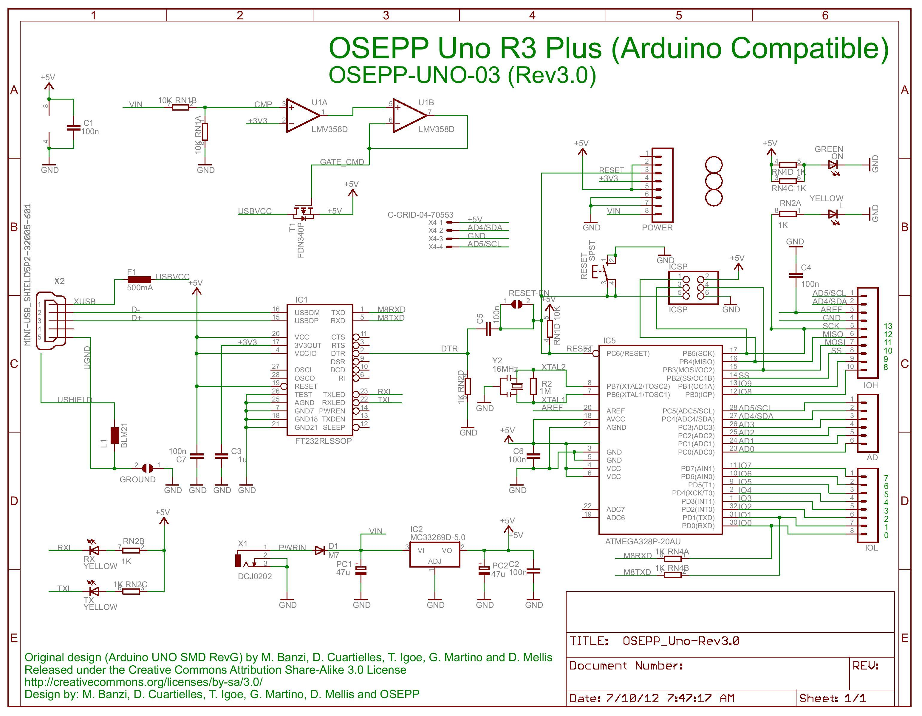 - 萬孔板正面元件位置圖 -  - 萬孔板背面走線圖 -  ## 影片 * [燒錄BootLoader](https://www.youtube.com/watch?v=smr9EddIL3Q) * [上傳程式](https://www.youtube.com/watch?v=cvyq-qohljg) ## 文章 https://www.instructables.com/%E8%87%AA%E9%80%A0%E4%BD%A0%E7%9A%84Arduino-UNO%E6%9D%BF/ https://www.microchip.com/en-us/product/ATmega328P#document-table https://www.electroschematics.com/diy-arduino-making-your-own-arduino/ https://makersportal.com/blog/2018/3/15/arduino-internet-of-things-part-1-burning-the-arduino-bootloader-onto-a-blank-atmega328p-chip-using-the-arduino-uno
×
Sign in
Email
Password
Forgot password
or
Sign in via Google
Sign in via Facebook
Sign in via X(Twitter)
Sign in via GitHub
Sign in via Dropbox
Sign in with Wallet
Wallet (
)
Connect another wallet
Continue with a different method
New to HackMD?
Sign up
By signing in, you agree to our
terms of service
.